This thread has been locked.

If you have a related question, please click the "Ask a related question" button in the top right corner. The newly created question will be automatically linked to this question.

UCD90160: Migrating the design from UCD90160 to UCD90160A.

Part Number: UCD90160

Hi Team,

We have a custom board, which has UCD90160 power sequencer to monitor and sequence the power rails of FPGA. In the new build of custom board, we have used a UCD90160A device which is pin to pin replacement device for UCD90160 . 

We have a system file(.tifsp file) of the design which has UCD90160 (added in the attached zip file for your reference). 

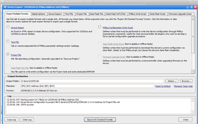
From this system file we exported the project file (XML file) of UCD90160 alone in the offline mode using Fusion digital tool as shown in below image (XML file is in attached zip file for your reference) 

In the new build of custom board which has UCD90160A, we imported this XML file to configure the UCD. 

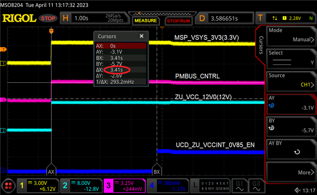
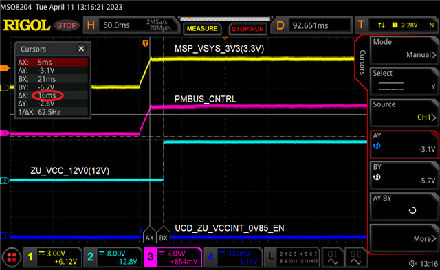
After successful import and configured, When the board is powered on, it is taking around 3.5 seconds to complete the power up the FPGA rails which was not observed in the previous boards which was used to power on immediately.  When started debugging the issue we found out that after monitoring the first voltage rail (i.e is 12V in our design which directly from a external supply), the enable to the second rail in sequence was delayed by around 3.3 seconds by the UCD. 

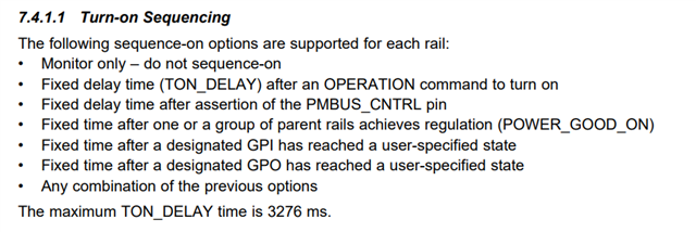
From the datasheet of UCD90160A, the max TON_DELAY for a rail that can be configured is 3276ms as shown below, which is almost matching the delay we observed as mentioned above.

By any chance UCD90160A is entering to Maximum TON_DELAY state to turn on the  second rail even though we have not configured the TON_DELAY of 3276ms?

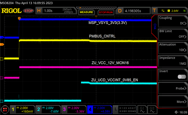
This delay in power up is observed only when the board is powered fresh. When the UCD is controlled through PMBUS_CNTRL pin to turn off and turn on the sequence without power off the external supplies, the UCD is behaving properly and we can observe the power up of FPGA rails happing immediately upon asserting the PMBUS_CNTRL without such huge delay. 

 Can we know what can be the factors causing such issues? 

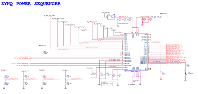
Here is the schematics of the UCD9016A for your reference 

UCD90160A_TI_query.zip

--

Thanks in Advance

Kiran

  • HI

    I did not follow you question. in your configure file, the PMBUS_CONTROL is the signal to trigger the ON/OFF.

    What do you mean power from fresh?

    Regards

    Yihe

  • Hi Yihe, 

    Sorry for making you bit confuse. I mean to say when we power on the board for the first time i.e., powering on the external supply to the board which power the UCD and other Peripherals (similar to cold start condition). In this condition we are observing the mentioned delay. This is condition where all the external supplies are ramped up for the first time( like 3.3V powering the UCD and 12V which is the first rail to be monitored).  

    Once the UCD powers up all the rails for first time, and next time when we try to turn ON and turn OFF the FPGA rails using PMBUS_CONTROL control(i.e., without doing power cycle of external supplies), we are not observing the delay. In this condition, UCD powers off all the rails in the sequence but the 12V rail which is the first rail to monitor will be still present because its from external supply and in our configuration UCD only monitors this 12V to start the actual power ON sequence and in power OFF sequence all the rails are powered OFF  in sequence but 12V will be still present. 


    --

    Regards, 

    Kiran

  • Hi

    I do not see how UCD can behave different without external event.

    1.you have to make sure that 3V3 is good

    2. the PMBUS_CONTROL need be a right postion so that UCD can turn on the powers.

    Please provide a waveform with 12V, 3V3, PMBUS_CONTROL and ENABLE signal from the first rail to be on.

    Regards

    Yihe

  • Hi Yihe,

    Here are the waveforms 

    1. When the board is powered on for the first time with external supplies

    Here we can observe the delay of around 3.4s between the 12V UP and the enable for the first rail to be turned on

    Zoom in version of first image shows the UCD power (MSP_VSYS_3V3) and PMBUS_CNTRL are ramped up on same time and the 12V is ramped up after around 16ms secs of delay in between.

    2. When we are deasserted and asserted the PMBUS_CNTRL (i.e., without doing power cycle and just controlling the PMBUS_CNTRL pin)

    Here we can observe that enable to the first rail to be turned on is HIGH at the time PMBUS_CNTRL pin is asserted without any huge delay as we seen in first case.

    --

    Regards,

    Kiran

  • Hi

    Thank you for the waveform.

    I can not explain unless more data is provided

    1. The probing need be directly from the UCD side to avoid any soldering issue. is the 0V85_En and 12V signals direct from Pin 11 and Pin 54.

    2. for the 0.85v rail. please change it to auto instead of control pin to see how it work

    3. for the 0.85V, please remove the 12V dependence after step 2.

    Regards

    Yihe

  • The probing need be directly from the UCD side to avoid any soldering issue. is the 0V85_En and 12V signals direct from Pin 11 and Pin 54.

    Hi Yihe, 

    The below capture is probed directly from the UCD pins. There are no change in the waveforms. Also, Soldering touch up to each pins of UCD was performed to avoid soldering issues.

    for the 0.85v rail. please change it to auto instead of control pin to see how it work

    3. for the 0.85V, please remove the 12V dependence after step 2.

    Making only 0.85V rail turn on configuration as auto (as none in configuration settings ) and all other rails as control pin, will there be any changes in the power on sequences of other rails with resect to 0.85V? Just wanted to confirm so we are not missing the power up sequence in any case.

    --

    Regards,

    Kiran

  • Hi

    Yes, that's correct. we only care 0.85V now so that you can keep the other rail off(not flip the control pin)

    Regards

    Yihe

  • Hi Yihe,

    We replaced the UCD90160A with UCD90160 and the issue got fixed.  We were in between one more debug where our MSP_VSYS_3V3 was slowly dipping when we were configuring the FPGA. we have a FPGA 3.3V rail (rail 7 in our UCD config) powering from TI's load switch whose input is MSP_VSYS_3V3. when the load was increasing, the voltage was slowly dipping to 3V. Due to this our UCD90160A was running into power cycle when the voltage dips below 3V and was resequencing the power rails and causing the FPGA to power cycle. And also we were not able to see any logs for the Under voltage fault for rail 7 in the UCD logged faults. 

    We tried powering the 3.3V (MSP_VSYS_3V3) from different power supply but then UCD was not yet all getting detected when powered from different source. So we wanted change the UCD device and we changed it to UCD90160. Now the 3.5sec start up delay has been fixed. But we could not able to identify what was the cause for such delay and also what are the changes to be taken care when we import the project file(XML) generated from UCD90160  into UCD90160A. 

    The 3.3V voltage dip is still present and will raise the separate query under the respective load switch part.

    Thank you.

    --

    Regards,

    Kiran 

  • Hi

    If your VCC is below 2.9V, UCD90160A will not function but UCD90160 can if brownout feature is not enabled. This is the difference.

    But i do not get why powering 3v3 from other source can prevent UCD being detected. Are you sure 3V3 is connected to the UCD?

    Regards

    Yihe

  • Hi Yihe,

    Thanks for the information. 

    Are you sure 3V3 is connected to the UCD?

    Yes, surely it was connected to UCD. There are other devices on the same rail like MSP430 which were all coming up when powered from other power source. 

    --

    Regards,

    Kiran

  • Hi

    You have to make sure V33, RESET, BPCAP, TRST are all good.

    Regards

    Yihe