This thread has been locked.

If you have a related question, please click the "Ask a related question" button in the top right corner. The newly created question will be automatically linked to this question.

TPS23770: Secondary side MOSFET failure.

Part Number: TPS23770

Hi,

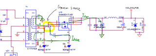
We are facing an issue with our PoE design, where the secondary MOSFET is failing(source to drain short) in the isolated flyback buck converter topology. 

When we measured the U19 MOSFET's drain and gate, we observed spikes in the voltages. 

Attaching both the schematic snip and the oscilloscope images for your reference.

What might be the root cause for the failing MOSFETs?

Thank you in advance.

PoE Design MOSFET Short Issue.pdf

  • Hi Alen,

    Thanks for reaching out to us!

    I think it may caused by the common source inductance/resistance that shared by both power loop and gate drive loop. Also transformer winding's leakage inductance could cause overshoot too.

    I saw you have two BZX84C18-7-F 18-V zener diodes here. They should help to clamp the Cgs voltage.

    Best regards,

    Diang

  • Hi,

    Thanks for your reply.

    So is this overshoot causing the MOSFET (U19) to fail?

    If yes, is there any way to overcome the issue?

    Regards,

    Alen

  • Hi Alen,

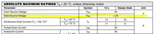
    If the Vgs waveform is true (neglect the noise coupling to the probe), it may damage the gate oxide as the overshoot is higher than 20 V. 

    Could you also measure the Drain-Source voltage of U19? And you may try to add a RC snubber to absorb the energy stored in the leakage/stray inductance, so that there may have less voltage overshoot. 

    Best regards,

    Diang

  • Hi Diang,

    Attached the Drain-Source voltage snip of U19 for your reference.

    We tried RC snubber with the values of 10 ohm  & 2200pF which was already suggested by TI, but we didn't observe any improvements in the waveform. So, kindly suggest some other  RC snubber values to overcome this.

    Regards,

    Alen

  • Hi Alen,

    SI4840DY-T1-E3 is rated at 40 V, and it is better to limit the voltage less than 80% - 90% of the rated value.

    The RC snubber circuit is used for alleviate the Vds(off) overshoot. It could be related to the stray inductance depending on layout and transformer leakage inductance. Power stage designer user guide has some calculation (www.ti.com/.../slvubb4b.pdf), but in fact the RC values needs to be adjusted in practical test sometimes. 

    The RC snubber needs to be placed with the FET with minimum path length to reduce the stray inductance too. You may increase C or reduce R slightly to see if anything could be improved.

    Best regards,

    Diang

  • Hi Alen,

    Since we have not get your response for a relative long time, I will close this thread for now. Please reply or open a new thread if you have further questions.

    Best regards,

    Diang