


hello
the datasheet said
8.10.1 CTLx Sequencing
The device has six control-input pins (CTL1–CTL6) to control six SMPS regulators, three LDO regulators,
and three load switches. This allows the user to define up to six distinctive groups, to which each VR can
be assigned for highly flexible power sequencing. Of the six CTLx pins, CTL3 and CTL6 can be configured
alternatively to active-low sleep enable pins. For instance, if a system level SLEEP state is defined such that
BUCK1 output regulation voltage is lower than in the normal mode, then BUCK1 SLEEP state can be assigned
to CTL3 or CTL6. By being pulled low, either CTL3 or CTL6 can be used to put BUCK1 into SLEEP state,
and BUCK1 will regulate its output at a voltage defined by BUCK1_SLP_VID[6:0] in Section 8.13.23. For a
demonstration of this feature, Figure 8-24 shows how BUCK1 is enabled from the CTL1 pin.
but how to define those VR groups? I could not find the corresponding registers, we plane to use TPS6508640, and there is a example as follows.
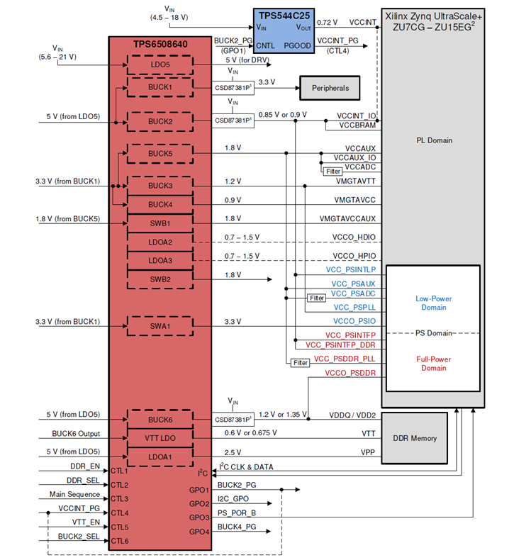
ddr_en -> ctrl1
ddr_sel->ctrl2
Main_sequence -> ctrl3
VCCINT_PG ->ctrl4
VTT_EN->ctrl5
BUCK2_SEL ->ctrl6
but where are those controls from? can I use MIOs of ZU MPSOC to genertate these signal?
