This thread has been locked.

If you have a related question, please click the "Ask a related question" button in the top right corner. The newly created question will be automatically linked to this question.

TPS61178: Device overheats

Part Number: TPS61178

Hi Team,

Our customer built a PCB with TPS61178 to step up the voltage for a USB charge board. The specifications are as follows:

Vin = 3V-13.5V
Vout = 18V
Iout = 1A

He copied the schematic diagram from Webench and built the PCB from the schematic. However, the device overheats and 2 of 5 devices were damaged with SW pin shorted to ground. He also added,

The only component I changed was the inductor, due to availability. The original inductor that webench included was a 2.5uH inductor. I changed it to a 2.2uH inductor, with a 2mOhm DCR and 15A rating

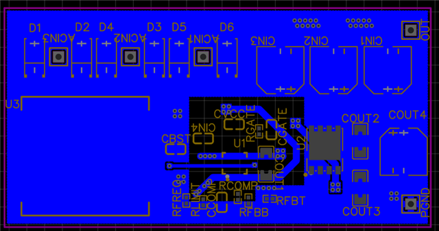
Since the pin width and copper trace width are 0.254mm for the SW pin, I routed a copper trace out of the other side as well, then used a via to the bottom layer to route another trace to the Inductor. I did this to add more

copper area, wasn't sure if it needed it. That's why the SW pin has copper coming out from either end. I also added a 3 phase bridge rectifier and 3 capacitors to power the circuit, but I've been powering the board with a DC regulated supply for testing purposes

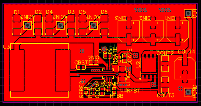
Aside from lack of vias and insufficient ground plane, do you find other design error?

Regards,

Danilo

  • Hi Danilo,

    It looks that your either end copper is acceptable and no more error exists.

    Could you please have a test of the SW stress and inductor current?

    Usually, the MOS is damaged due to overvoltage or over current.

    Please use minimum loop and maximum bandwidth to do the stress test.

    And you can series in a line with the inductor to test the inductor current.

    Best Regards

    Fergus

  • Hi Fergus,

    Thank you for your response. Here is the update from our customer.

    So far, I've tested input current, current between the SW pin and the inductor, and the output current.
    Here's what I'm getting while powered with 12V and supplying power to a USB Type-C charge module (what it's intended for):
    (This is while charging a smart phone)
    Input: 0.75A @ 12V
    SW pin to the inductor: 0.74A @ 12.3V
    Output: 0.5A @ 17.8V
    (This is while charging an iPad)
    Input: 2.51A @ 12.0V
    SW pin to inductor: 2.68A @ 12.17V
    Output: 1.41A @ 18.0V
    All of the boards very hot, but one of them does worse than the others! The majority of the heat is coming from the inductor and the TPS61178. My input diodes are also getting warm, but not hot like the latter two are.
    Overall I am losing around 4.74W to heat when charging the iPad, but hardly lose any power to heat when charging the phone.
    However, once I lower the input voltage, the performance decreases sharply. I'm only seeing efficiency around 67% when charging my phone. And I can't charge the iPad at lower voltages because it exceeds the current limit.
    Here's what I get when the input voltage is lowered to 6V:
    (Charging my phone)
    Input: 3.04A @ 5.78V
    SW pin to inductor: 3.01A @ 5.41V
    Output: 0.58A @ 18V

    Regards,

    Danilo

  • Hi Danilo,

    it looks that the device is overheated.

    1. the switch frequency seem too low, 715K means around 200k. the low frequency causes high peak current and high core loss for the inductor.

    Please change the resistor Rt to 200k to have a try.

    2. the device's loss is much more than expectation, one of the reasons may be the high temperature.

    you can first try to use a fan to cool down the device to see if the efficiency come to normal.

    for long term, it is recommended to use a 4-layer PCB to enhance the heat dissipation.

    Please tell me whenever customer has any feedback, especially the frequency change.

    we can get smoother communicate through email.

    Best Regards

    Fergus