This thread has been locked.

If you have a related question, please click the "Ask a related question" button in the top right corner. The newly created question will be automatically linked to this question.

TPS552882: MOSFET Selection

Part Number: TPS552882

Hi Experts, 

Could you please help to check the MOSFET spec which could be use for TPS552882 or not?

My application : 

Vin : 4.75~21V

Vout : 5V/3.2A

The Sch, component ref is Q16, Q18

The MOSFET Spec shown below.

Thanks 

  • Hi Alan,

    Thanks for reaching out.

    I have some questions need to check with you, please kindly reply:

    1. What is the application used here?

    2. Why 600kHz switching frequency is chosen since it is in AM band?

    3. Just curious, why do you put 0.1uF cap at PG pin, I see it is reserved for EMC, but when the device works in normal mode, the PG voltage would be stable and doesn't affect EMC I think.

    4. Recommend to leave C222 DNP for now.

    5. Recommend to change R199 to 20k.

    6. Recommend to separate AGND(for all signal pins: FB, COMP, MODE…) plane with PGND plane, and connect it at VCC cap.

    7. The MOS looks ok from my side.

    8. Please follow the layout guideline.https://www.ti.com/lit/pdf/slvaer0

    Regards,

    Bryce

  • Hi Bryce, 

    1. What is the application used here? Multi-port Type-c Hub

    2. Why 600kHz switching frequency is chosen since it is in AM band? No particular reason

    3. Just curious, why do you put 0.1uF cap at PG pin, I see it is reserved for EMC, but when the device works in normal mode, the PG voltage would be stable and doesn't affect EMC I think. Usually recommend by our EMC team. I don't think it will affect EMC, too. But just follow the team member's suggestions. 

    4. Recommend to leave C222 DNP for now. Yes, it,s DNP.

    5. Recommend to change R199 to 20k. OK.

    6. Recommend to separate AGND(for all signal pins: FB, COMP, MODE…) plane with PGND plane, and connect it at VCC cap. OK

    7. The MOS looks ok from my side. OK, thanks. Could you please provide some selection guide?

    8. Please follow the layout guideline.https://www.ti.com/lit/pdf/slvaer0

  • Hi Alan,

    Thanks for feedback.

    About MOSFET selection, we mainly consider the Vgs(th), Vds_limit, Vgs, Id, Rds_on, Pd, tr, tf and package(thermal), you can refer to below calculation tool for MOSFET efficiency calculation when MOS specs are input in.

    Regards,

    Bryce

  • Hi Bryce, 

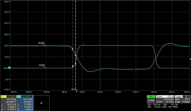
    Below is the Waveform of High Side MOS VDS and Low Side MOS VDS. 

    Vin : 20V, Vout : 5V, 3A.

    Does there have the risk of shoot-thru?

  • Hi Alan,

    Can you probe the DR1H, DR1L and SW1 waveform as below, so that we can see what is the real dead time now, we can’t see it from the below picture. Please (1) use BW=500MHz voltage probe; (2) turn off the scope channel BW limit; (3) change the SW1 voltage scale to 0.5V/div.

    Also, it’s better to probe Vin voltage, add 20V offset at the channel and see if Vin decreased during the dead zone and if there is shoot through happened.

     I will also look into the layout if there is any risk.

    Regards,

    Bryce

  • Hi Bryce, 

    Please see my waveform. 

  • Hi Alan,

    Thanks for waveforms, what is the H-VGS signal? It doesn't make sense of the high voltage value of 17V+18.5V=35.5V, if SW1=20V, the Vgs voltage would be 15.5V which is not correct.

    Do you use the same MOSFET for low and high side FETs? Why is the rising and falling time of H-VGS so long? And L-VGS is fast as I see.

    Regards,

    Bryce

  • Hi Bryce, 

    The test environment seems to be something wrong and I didn't notice that. 

    I've already re-set up the test environment. Please see the waveform. 

    The H/L mosfet is the same. 

  • Hi Alan,

    Thanks for waveforms.

    I still see the Voffset at each channel, is it the scope mistake?

    From the waveforms, as you can see, there is a delay between DR1H falling and SW falling due to toff time>ton time of MOSFET. And after the internal driver dead time, DR1L rises. I think there exists risks when SW is falling to zero(high side not totally turns off but low side turns on), and in some cases, the dead time becomes smaller which could cause the shot-through time gets larger and finally FET damaged.

    From the waveform below, you can see there is two negative dips of SW waveform(red), that is the dead time and it can make the shot-through not happen.

    Regards,

    Bryce

  • Hi Bryce, 

    Thanks for your detailed explanation.


    Thanks a lot. 

  • Hi Bryce, 

    If we want to solve this issue, Could we change the high-side mosfet with a shorter Td(off) ?

  • Hi Alan,

    I think it's better to choose MOSFET (both high side and low side) with lower Qg with smaller tr and tf spec(tr and tf should be more symmetrical).

    Regards,

    Bryce

  • Hi Alan, 

    We have not seen an update from you for four weeks, so I assume the questions are answered.

    I close this thread now. If there is still something open, please reply and the thread will get opened again.

    If you have any other question or of the thread has been locked, please open a new one.

    Best regards,

    Bryce