Hi,TI expert
We need your technical support for our product: Buck power optimizer.
1. Schematic review.
2. UCC27282 damage issue @ 98% duty, 120k Fsw, 16A loading.
May I have your email? I can send schematic for review.
This thread has been locked.
If you have a related question, please click the "Ask a related question" button in the top right corner. The newly created question will be automatically linked to this question.
Hi,TI expert
We need your technical support for our product: Buck power optimizer.
1. Schematic review.
2. UCC27282 damage issue @ 98% duty, 120k Fsw, 16A loading.
May I have your email? I can send schematic for review.
Hello Terry,
One way to share information and not be on a public forum, is to submit a friend request. Once we have completed the friend request we can communicate and share information in private.
Regards,
Actually, i think this is a basic question for datasheet, and we can talk here, right?
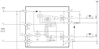
I have read this chapter, but cannot understand this chapter completely, so could you show me where to place 2ohm resistor and leakage Zener diode in the simplified application diagram? and expain why they can protect the chip?
Thanks again.
Hello Terry,
I send you a friend request, let me know if you receive the notice. I clicked on your name and options were available to connect, I assume your view is similar.
The paragraph you show is for general guidance on how to protect the IC pins. The 2 ohm resistance is in reference to adding some protection to the HS pin if excessive negative voltage may be present. Below is an example of where to place the resistor, on the HS pin before the connection to the HB capacitor and Mosfet common source and drain.
For the zener diodes, this is referring to adding zeners to VDD and ground, or HB and HS or maybe LI/HI and ground (VSS), if you expect to exceed the device voltage ratings on these pins.
Regards,
