This thread has been locked.

If you have a related question, please click the "Ask a related question" button in the top right corner. The newly created question will be automatically linked to this question.

LM5146: Overcurrent on start up - bad switch node waveform

Part Number: LM5146

Hi,

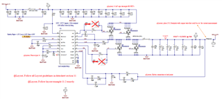
I have a LM5146 based design.  The design was done in TI Webench and initial evaluation was done with the LM5146-Q1-EVM12V.

The design inputs are very similar to the LM5146-Q1-EVM12V, however the output voltage is slightly higher at 12.5V and the output current is 25% greater at 10A.

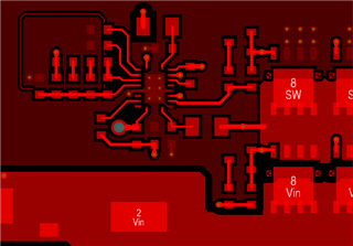
The layout closely follows the TI recommended layout in section 11.2 of the part datasheet.

The key differences that Webench changed for the higher current were:

  • Paralleling of two additional FET's
  • Different inductor value and size
  • All of the compensation network values

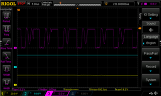
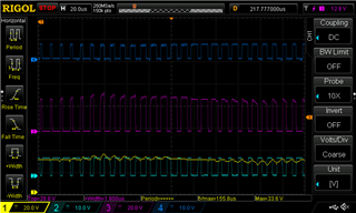
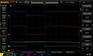
When I start to bring up the supply, with no load attached, the supply audibly "sings" and the input supply overcurrents and sags the input voltage. Connecting a scope to the switch node shows that the low side FET appears to be turning on with the high side FET on. Waveform and Webench design attached. 

Magenta is switch node, Blue is output voltage (target is 12.5V), yellow is input voltage (initially 30V at 3A) 

Thanks in advance for your support...

WBDesign141 (1).pdf

  • Hi David,

    Can you share your actual updated schematic?

    Also can you attach the excel calculator 

    https://www.ti.com/tool/LM5146DESIGN-CALC 


    It looks like both of your FETs are turning OFF, and SW node is ringing around VOUT.

    This is normal for diode emulation.

    You can check if the FETs are both on (cross-conduction) by checking HO and LO.

    Are you starting up into full load or no load? Does this happen at no-load?

    For 12.5V 10A (125W) output, you need 4.6A at 30V (assuming 90% efficiency)

    Hope this helps,

    -Orlando

  • Hi Orlando,

    Thanks for reviewing my design.

    This is with no load, as another point of reference this current limited supply easily powers up the Eval board with no load attached as well.

    My schematic is attached, I will download and fill out the Excel sheet and post when finished, I had not previously used that tool, I was using the webench design I attached.

    Based on the loud audible noise, and current sag of the input supply, I am fairly confident that the half bridge FETs are both on.

    Also, I have tried powering the LM5146 both at the intended input and at TP2 after the EMC filter with the same results.

    Thanks.

  • Hi David,

    OK got it. Can you probe HO and LO at the FETs so we can confirm?

    Also confirm your LO resistor is 0Ω.

    Your HO and LO traces from the FETs to the IC should be sort length and 20mil thick to minimize parasitic inductance and resistance.

    Are you able to test with single pair FET? Use the pair closest to the IC.

    Let me know,

    -Orlando

  • I probed the HO and LO drives, attached are the waveforms, the magenta is still the switch waveform, however with the probes attached it appears to look more like it should, the current load on the bench supply is still high for no-load but is not tripping,we did increase the current limit to 5A on the bench supply.

    They are in order, the dark blue is HO relative to the switch node, light blue is LO relative to gnd. The yellow is the input voltage.

    The supply still makes audible noise. We discovered that by changing the leads from the bench supply to minimize resistance and inductance we could change the magnitude and frequency of the audible tone. also by including and removing the input filter.

    close up shots of the HO, SW, and LO show there is dead time. I am going to use the Excel sheet you linked in the first post to review the compensation network and then tomorrow plan to remove two of the four FET's.  The resistors were confirmed to be zero ohm. The HO and LO traces from the FETs to the IC appear reasonably short and fat.

    other than the loud audible sound it appears closer to what I would expect, the bench supply says 0.4A @ approx 30V or 12W with no load. We have not tried to let it run for more than a few seconds at a time, just enough to capture the waveforms and attempt to look at thermals.

  • Going back and reviewing the Webench design attached to my first post, M2 specified is a BSC240N12NS3 G, which is obsolete, I used the same FET as the top side, it has slightly higher gate charge, what FET, that is in stock would you suggest?

  • Hey David,

    What is your inductor part number?

    Double check your inductance matches the quickstart recommendation.

    The input filter needs to be damped, you need an bulk capacitor with ESR if youre using the EMI filter.

    https://www.ti.com/lit/an/snva538/snva538.pdf

    However if you bypass the inductor this shouldn't matter.

    Your VIN seems to be reacting to SW node way too much, it clearly dips when SW turns on and rises when SW turns off. 

    For 20V/div its basically a 5V drop it looks like.

    Are you able to probe inductor current? You'll need to add a wire on the VOUT side of the inductor and use a current probe.

    Regarding FETs, Optimos6 FETs are pretty good:

    https://www.infineon.com/cms/en/product/power/mosfet/n-channel/optimos-and-strongirfet-latest-family-selection-guide/

    https://www.infineon.com/cms/en/product/power/mosfet/n-channel/isc060n10nm6/ for lower QG (high-side)

    https://www.infineon.com/cms/en/product/power/mosfet/n-channel/isc027n10nm6/ for lower RDSON (low-side)

    Let me know inductor part number,

    -Orlando

  • Hi Orlando,

    The main Inductor is the SER2918H-223KL,  Not sure if you saw it but I had attached the entire Webench design to the first post, it includes all design inputs and the BOM.  If you can share your email I can share the design directly with you.

    I assume by quick start you mean the Excel design tool you had linked, and it matches

    Your observation regarding input capacitance matches an observation a co-worker made last night comparing my designs capacitance, what Webench placed, with the datasheet recommendations for minimum capacitance.   

    Although I am still not sure if the input voltage ripple is an artifact of the converter not operating properly or is a potential cause of the converter not operating properly.

    With regards to your recommended FET's, I had seen those but had ruled them out as they are only 100V parts. My design can operate up to 90V.  Regardless, I do have some flexibility in this first iteration for max operational voltage so I will lower the input spec and test with those parts. 

    Thanks,

    Dave

  • (I am Dave's colleague) The geometry of gate traces is as follows:

    HO- 14 mils wide,  820mils to series resistor, then 230 mils to first FET, 480 mils to second FET
    LO-  14 mils wide, 350 mils to series resistor, then 160 mils to first FET, 380mils to second FET

    Stackup is 6 layers, with 10 mils from above traces to ground planes

  • Orlando, Excel sheet attached. The compensation values calculated by the sheet are substantially different than those provided by Webench, we are changing them now...

    Interface board PS.xlsm

  • success! setting the compensation network components to the values generated by the Excel sheet design tool VS the values generated by Webench resolved the issue, no audible noise and the bench supply drops to zero amps out with no load on the switcher.  

  • David,

    Awesome, glad to hear its working.

    The compensation depends heavily on the output capacitance, the webench had much smaller output capacitance and tats why the compensation was different from Quickstart.

    Let us know if you need further support.

    -Orlando

  • yep, of course, thanks for your help...