This thread has been locked.

If you have a related question, please click the "Ask a related question" button in the top right corner. The newly created question will be automatically linked to this question.

LM5146: Layout Review

Part Number: LM5146

Hi Team,

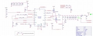
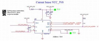
We are using the LM5146RGYR Switcher part in our Layout Board file. I had attached the images of the Board file and Schematics. Please review the layout and share your feedback with us.

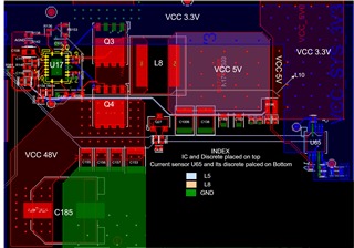
The PCB we are using is of 12 Layers:

IC - Place on top

Current sensor and its discrete are placed on bottom

Layers 2,4,9 and 11 are Ground.

Thanks and regards

- Teja.

  • Hi Teja,

    Heres my feedback:

    Looks like you have two different pull-up for PG, using VOUT and VCC.

    Increase your HO and LO , and SW trace thickness to 20mil. Also, it's best for HO and SW to route together, closely coupled.

    I don't think you need the ferrite bead on VIN, beads are typically for MHz level noise, this IC should need that high-frequency filtering. Simply placing the VIN cap close to the pin should be sufficient.

    No need for resistor to connect AGND to PGND, a net tie should do it as a copper connection in the PCB. See figure 11-2 in the datasheet, and also LM5146-Q1-EVM12V layout design.

    Everything else looks good to me,

    -Orlando