


-----------------------------------------------------------------------------------------------------------------------------------------------------------------------------------------------------------------------------------------------------------------
e2e.ti.com/.../4604724
-----------------------------------------------------------------------------------------------------------------------------------------------------------------------------------------------------------------------------------------------------------------
First ask the questions and answer the content, there are still some things that I don't understand, and I need to ask for your help.
I don’t quite understand the content of the reply to [Q4] in the previous article. Could you please describe the POR mechanism of this connection method in detail?
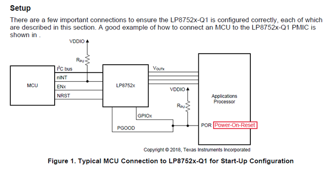
[Q4] In the application setting in Figure 1 above, both GPIOx and PGOOD are connected to POR (power-on reset), is it for dual reset control?
*GPIOx => MCU controls GPIOx to reset the next-level application processor through I2C commands.
*PGOOD => When the PMIC output voltage or output current is abnormal, PGOOD outputs low level and resets the next-level application processor.
---------------------------------------------------------------------------------------------------------------
*The following are newly added questions
1) Default OTP configuration for Function PIN - EN2 (GPIO2), EN3 (GPIO3):
GPIO2_SEL= 1 => GPIO2
GPIO2_OD = 1 => Open-drain output
GPIO2_DIR = 1 => Output
GPIO2_OUT = 1 => Logic high level
GPIO3_SEL= 1 => GPIO3
GPIO3_OD = 1 => Open-drain output
GPIO3_DIR = 1 => Output
GPIO3_OUT = 1 => Logic high level
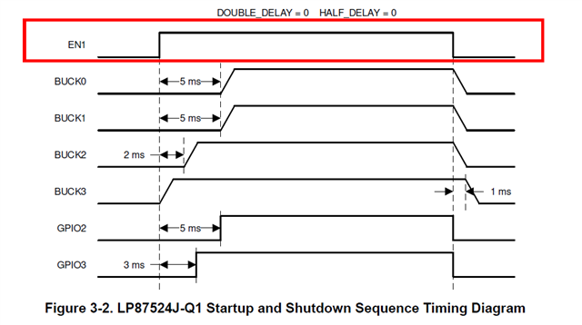
In the timing sequence of Figure 3.2 above, GPIO2 and GPIO3, which are set as GPIOs, are enabled by EN1. When EN1 pulls "H", GPIO2 and GPIO3 are enabled in sequence after waiting for a delay, and start to output, and the output level It is determined by the register settings GPIO2_OUT and GPIO3_OUT.
[Q1-0] Is there any mistake in the above understanding?
[Q1-1] After these two pins are set as GPIO, if logic control is required, who is the master controller? (Is it PMIC?)
[Q1-2] If the settings in Figure 1 above are taken as an example (the MCU is connected through I2C, and the GPIO of the PMIC is output to the next-level application processor):
The GPIO control method can be controlled by the MCU through I2C to output digital level "H" or "L" to the next-level application processor by controlling GPIO2 and GPIO3? Or is there another control method?
