This thread has been locked.

If you have a related question, please click the "Ask a related question" button in the top right corner. The newly created question will be automatically linked to this question.

TPS25750: How to use ADCINx pins of TPS25750D

Part Number: TPS25750

Dear TI team


I have a question about "Table 9-5" in the datasheet.

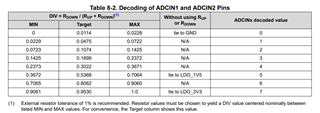
It seems that the mode setting changes depending on the combination of decoded values of ADCIN1 and ADCIN2.

I do not understand the relationship between the meaning of numerical values such as Decode value "7,5,2,1" and the AD input value.


So I checked the thread below.

https://e2e.ti.com/support/power-management-group/power-management/f/power-management-forum/1160350/tps25750-how-the-adcinx-pins-are-decoded?tisearch=e2e-sitesearch&keymatch=TPS25750%2525E3%252580%252580decoded#

https://e2e.ti.com/support/interface-group/interface/f/interface-forum/1079560/tps25750-where-istps25750-adcin1-and-adcin2-voltage-configuration-table?tisearch=e2e-sitesearch&keymatch=TPS25750%252525252525E3%25252525252580%25252525252580ADCIN1#


Although it is not mentioned in the datasheet, I referred to the diagram in the above thread.

Is it correct to understand that the calculated value of "0 to 7" can be obtained by inputting the value of "target" x 3.3V to ADCIN1/ADCIN2?

(The TPS25750 LDO_3.3V pin output can be divided down and connected to ADCINx.)


Also, please tell me about setting the TPS25750D as a "sink".

Should I select "Safe Mode" if I load the patch from EEPROM and do not want to enable power path until negotiation is complete?

Please let me know if I'm missing something.


Best Regards,

Taroimo

  • Hi Taroimo,

    Yes you are correct there is a table missing from the data sheet for the decoded values. I will elaborate on how the ADCINx pins are used to setup TPS25750.

    The ADCINx pins use a decoded value based off 3 different charts in order for you to understand how the device will behave in different environments. The first table you will use is actually the one that is missing, see below:

    This chart will tell you your decoded value on the ADCIN1 and ADCIN2. These decoded values are dependent on resister divider tied to your pins when being tied to LDO3V3. For instance, if you have a .50 resistor divider connected to LDO 3V3, your decoded value would give you 5. Once you have your decoded values for both ADCINx pins, you can use the pin strapping chart to determine default behavior and the I2C address setting chart to determine your slave address for the device.

    You are also correct here, if you are loading configuration from an EEPROM, you would want to use SafeMode which will keep the device in patch mode and not enabled any sink path until the configuration is loaded. 

    Regards,

    Brandon

  • Hi Brandon,

    Thanks for the quick explanation.
    Please tell me one more thing.
    There is a description of "Note that the configuration could put the device into a source-only mode." in the description of SafeMode in Table 9-5.
    In what cases does a device end up in unintended "source-only mode"?
    I am aware that it can be set as DRP or sink-only even in SafeMode.

    Best Regards,
    Taroimo

  • Hi Taroimo,

    The dead battery configuration is geared towards how you boot and load your configuration. Once you load you configuration, which contains your power role status and preference, the device will operate based off of that configuration. For example, if you are in AlwaysEnableSink, you will always enable the sink path even before a configuration is loaded. Then once the configuration is loaded, the device can become DRP, source-only, or sink only.

    Regards,

    Brandon