This thread has been locked.

If you have a related question, please click the "
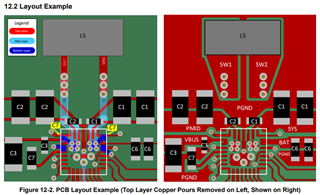
Ask a related question" button in the top right corner. The newly created question will be automatically linked to this question.

BQ25792: Single sided layout recommendations and ESR requirements

Part Number: BQ25792

Hello, we have a 3S lipo charging board using the BQ25792 chip. Do to the mechanical constraints all the components have to the placed on one side. What are the layout guidelines for a single sided layout to maximize power output? Currently we are able to achieve a charge current of 3A without active cooling, but want to push that as far as possible.


We also are using polymer capacitors for increased vibration resistance, but are seeing intermittent failures of the charger chip. Once charge is enabled, the chip fails and shorts PMID to ground. What is the maximum recommended ESR on the PMID and SYS pins? Currently the the 0.1uF cap is ceramic to be placed as close as possible to the IC, but the 10uF polymer caps are big (2312, 6032 metric) so the total area the to the last cap is large. Could this or the use of polymer tantalum capacitors cause the issue? The board powers up fine, but once a battery is plugged in and charge is enabled the chip fails.

  • Hi Peyton,

    Below is the datasheet recommendation for a 3 layer board:

    We do not have a recommend 2 sided (top and bottom) layout.  Some customers have been able to get such a layout to function.

    The 3 layout layout above minimizes switching noise and maximizes power dissipation. To minimize switching noise, the IC and the two 0.1uF SYS and PMID capacitors must be placed on the same side as the IC to filter switching noise.  It is also highly recommended to place the SYS and PMID bulk capacitors on the same layer.  The inductor can be placed on the bottom side with SWx pin vias under the IC (so that the SYS and PMID capacitors on top side have a direct connection to IC GND).   To improve IC efficiency, I recommend using fsw=750kHz and 2.2uH inductor.

    Regards,

    Jeff

  • Sorry for the confusion, but we have a 4 layer board. The components must all be placed on the same size. In the data sheet example there are two capacitors placed on the bottom side (C7), and am wondering if there is a recommended layout for those to be on the top layer. I am following  the recommendations you mentioned from section 12.1 in the data sheet, but am seeing failures. Are there recommended ESR maximums for PMID? Could the  larger loop from big polymer tantalum capacitors create the failure mode we are seeing? 
     

  • Hi Peyton,

    The capacitors need to be very low ESR (<<50mohm) in order to ensure loop stability.  

    The most common failures are from hot plug at the input > 15V supply or hot plug of 4S battery at BAT.  An input RC snubber and BATP capacitor or TVS diode might be required.

    Regards,

    Jeff

  • Okay, thank you! I will make these changes and test further.