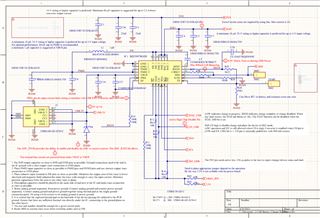
Hi everyone.
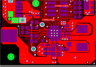
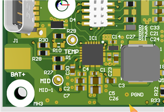
The BQ25887 IC is heating up while its charging on 1.2A from USB. The circuit is exact the same as the development board as shown below
Hi everyone.
The BQ25887 IC is heating up while its charging on 1.2A from USB. The circuit is exact the same as the development board as shown below