This thread has been locked.

If you have a related question, please click the "Ask a related question" button in the top right corner. The newly created question will be automatically linked to this question.

BQ76952: REGIN

Part Number: BQ76952

Hi,

I am using BQ7659203 SPI comm support devices and facing following issue

(1) applying 5.0V at REGIN pin and not using any LDO FUNCTION of this device and not using any TS!/TS2 pin, whenever i am plugging cell connector before giving +5V externally ,its damaged means

its VREF 1.8 V o/p is not build .

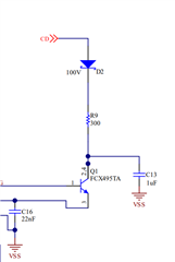
(2) if i am using this suggested supply ,output at VREGIN is approximate 6.0 V ,Is OK or require to reduce this , transistor is MMBT5551 
Please suggest ...it is urgent .

  • Hello Ramesh Gupta,

    whenever i am plugging cell connector before giving +5V externally ,its damaged means

    Can you please elaborate more on this? I am not sure what you mean by damaged. 

    The device contains one internal LDO (REG18) and two external LDOs (REG1 and REG2). The REG18 is used for internal circuitry and does not depend on the voltage of the REGIN pin. On the other hand, the REG1 and REG2 LDOs do need REGIN to be 5.5 V and above to function properly, and these are used for external circuitry purposes. 

    What is the issue you are facing and what are you trying to do?

    If using the suggested circuitry for the BREG Pin and REGIN, please follow this.


    Regards,
    Jose Couso

  • Dear Sir,

    I am using external +5V VCC and if i am giving AFE Input using Cell Voltage sensing connector in my pack directly without giving +5V at REGIN

    device is not communicating with MCU and i have observed that VREG18 output is 0.

    This thing happens lot of time with actual cell Input connector. 

    After replacing BQ chip communication is started with MCU.

    I am following the below step,

    (1) First give +5V at REGIN and our MCU then connecting the Cell Input Connector, No Issue observed.

    (2) if I am connecting directly cell input to AFE with +5V then its device failure maximum times.

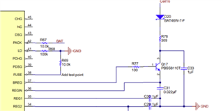
     Please check the schematic and suggest modifications.

    OGOBMS.docx

  • Hello Ramesh,

    First give +5V at REGIN and our MCU then connecting the Cell Input Connector, No Issue observed.

    The BQ7695203 uses REG1 voltage for SPI communications (MISO uses REG1 voltage). If REG1 has 0V, then there will be no communication.

    So, when you power REGIN with 5V, you are feeding REG1 which is by default programmed to 5V in the BQ7695203. This is why no issues are observed.


    Is there a reason why you are using SPI specifically? We recommend to use I2C because it can do block reads and writes, so it makes it easier to read many registers in one transaction, like when reading cell voltages for example. We have instructions on how to go from SPI to I2C with the BQ7695203, let me know if interested. 

    i have observed that VREG18 output is 0.

    REG18 is zero volts when the part is in shutdown mode. Otherwise, it should be 1.8V at all times as long as the pack voltage is greater than the shutdown stack voltage threshold.

    Comments on the schematic:

    1- BREG pin: If this pin is not used and pin 36 (REGIN) is also not used, both pins should be connected to pin 17 (VSS). If this pin is not used but pin 36 is used (such as driven from an external source), then this pin should be connected to pin 36 (REGIN).

    2- C150 cap should reference to VSS directly to avoid VC1 to go below VSS.

    Regards,
    Jose Couso

  • Hi jose ,

    Thanks for your reply,

    Is there a reason why you are using SPI specifically? We recommend to use I2C because it can do block reads and writes, so it makes it easier to read many registers in one transaction, like when reading cell voltages for example. We have instructions on how to go from SPI to I2C with the BQ7695203, let me know if interested. 

    I am using isolated spi bus communication and i am going for production launch,

    any performance issue with with spi bus please elaborate

    i have observed that VREG18 output is 0.

    REG18 is zero volts when the part is in shutdown mode. Otherwise, it should be 1.8V at all times as long as the pack voltage is greater than the shutdown stack voltage threshold.

    how to check the fault in my board ,After replacing the chip with new chip communication is started again. 

    I am now using BREG  as recommended in datasheet and evaluation board but not using any of the ldo of this chip set. 

    if am using breg for VREGIN and measure the voltage it is going upto 6.0 V.


  • Hello Ramesh,

    any performance issue with with spi bus please elaborate

    No problems at all. Like I mention above, I2C can do block reads and writes. If you are ready for production, then nothing to worry about. I was just suggesting.

    how to check the fault in my board ,After replacing the chip with new chip communication is started again. 

    If it shutdown, the TS2 pin will read a non-zero voltage (typically 3.5V). When in normal operation, TS2 pin reads close to zero volts.

    I am now using BREG  as recommended in datasheet and evaluation board but not using any of the ldo of this chip set. 

    This is ok.

    if am using breg for VREGIN and measure the voltage it is going upto 6.0 V.

    This is normal behavior.


    From what I can gather from your reply, the part you were using was either damaged or in shutdown.

    Regards,
    Jose Couso

  • Thanks Jose,

    I think  that the device has been damaged , Can you suggest any improvement in our schematic so that i can protect my device from damage.

    Please Share the document how to change SPI to I2C.

  • Hello Ramesh,

    From the original question, improvement should be made on the BREG pin. Check that the voltage on the BREG pin does not fluctuate between 0V and 6V, it should be a steady voltage. Also, I recommend connecting BREG pin to REGIN directly.

    Reference to this E2E thread which goes in details about the abs max for BREG, LDOs, and REGIN pins

    Please see the SPI to I2C reference guide attached. 3644.bq76952_ReconfigureSettings.pdf

    Regards,
    Jose Couso

  • Hi Jose,

    I have been  remove external supply at VREGIN PIN and using  BREG for supply input at REGIN input

    using Vbatt+ in place CD, 

    any other suggestion

  • Hi Ramesh,

    using Vbatt+ in place CD

    This is fine. As long as there's voltage on VBAT, the LDOs will work just fine.

    any other suggestion

    I see you are using P-channel FET configuration for external balancing. There's nothing wrong with it, just wondering if there's a specific reason. 

    P-channel vs. N-channel balance FET selection may also be influenced by cell connection. During cell connection, inrush current through the filter resistors will turn on P-channel balance FETs and pull up the lower input. This effect can continue down the cell stack. N-channel FETs do not turn on during recommended connection and may be preferred. 

    If you have tested P-channel FET and works as expected, then you can move forward and ignore the comment above.

    Regards,
    Jose Couso