This thread has been locked.

If you have a related question, please click the "Ask a related question" button in the top right corner. The newly created question will be automatically linked to this question.

LM3489: Load regulation clarification when 20V/5A PD profile demand

Part Number: LM3489
Other Parts Discussed in Thread: TPS65988,

Hello TI team,

Good day !

We are using the TI PD controller TPS65988 for USB - C PD profile, we have two port design 1st port 100w & 2nd port30w.

For your reference ,kindly refer the previous case# CS1650250.

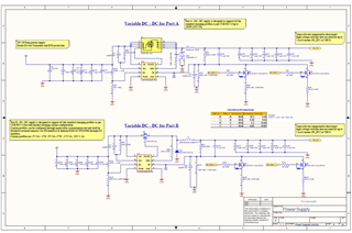
Attached schematic for reference, refer the page# 9. 

During the testing , we have observed the following and we have system cable which is of length 2.5 meters ,

 at NO-LOAD in board testing point measured 19.88V 

at full-load in board testing point measured 19V, why there is a drop of 0.88V between no-load and full load ?

at 2.5m cable end / device side measured 18.3V 

  • Hi,

    Thanks for utilizing our parts in your design. I've looped in the appropriate engineer who supports your part. 

    For now, it seems like what you are seeing is light-load operation where the LM3489 will deliver a pulse of energy to the output capacitor, and because it is light load, it takes a long time to decrease to the actual target value. Do you have any waveforms of switch node and VOUT at steady-state?

    Regards,

    Richard 

  • Hi,

    Are you measuring the output voltage right at the output capacitors (C65 and C79)  or after the long 2.5 meter cable?

    There will definitely be some I^R losses at full load across the 2.5 meter capable and that could be the reason the output is lowered than intended. 

    Regards,

    Jimmy  

  • Hello Jimmy,

    sorry for the delay in reply.

    I am measuring the voltage at board and device side.

    As I mentioned , 19.88V at board level in NO-LOAD and 19V at board level in full load.

    Thanks,

    Nithiyanantham.K

  • Hello Richard,

    Sorry for the delay in reply.

    Could you please specify at which load condition do you need the waveform of Switch node and VOUT?

    Can you be more specific on the location of switch node you can mark it in the schematic?

    Thanks,

    Nithiyanantham.K

  • What is the input voltage (Vin)? Are you making sure that at full load, the device is not operating in dropout condition? 

    You can check if it is in dropout by probing the SW node on the inductor primary terminal. 

    If the device is in dropout, the switching frequency should be folded back to a lower value then originally switching.