This thread has been locked.

If you have a related question, please click the "Ask a related question" button in the top right corner. The newly created question will be automatically linked to this question.

LP55231: Standby mode current consumption

Part Number: LP55231

Hi,

I have a battery powered low power application. during my device idle mode I get a current consumption of around 40uA. I'm running a test sequence where I:

Power On System -> (Wait 3 seconds -> Enable LED sequence with 2 LP55231 -> wait 3 seconds -> Disable the LP55231 by setting EN pin low -> wait 3 seconds) -> Repeat

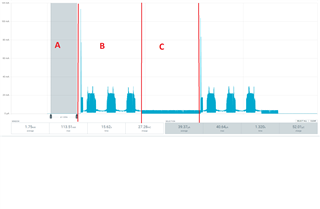
below is a screenshot of my power measurements. I've divided into 3 sections:

A: 3 seconds prior to enabling the LED sequence on the lp55231 on startup.  (40uA av)

B: 3 seconds LED is running (3.72mA Av)

C: 3 seconds after setting LP55231 EN pin to low (94uA Av) 

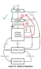
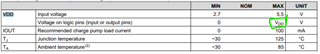
My expectation is that when setting EN to low both LP55231 should enter standby mode and have a current consumption of ~200nA but instead I'm seeing an additional 54uA.  I'm convinced it's the LP55231 that is the source of this additional current. if i leave all other parts of my firmware alone and just comment out the function that enables the LEDs i never see the current increase of 54uA.

Any idea why this is happening? Is there anything additional i should be doing beyond just setting the EN pin low?

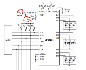
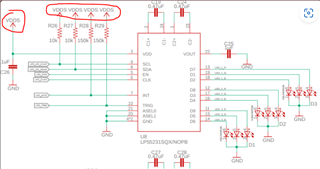
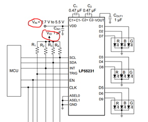
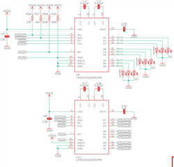
Below are some code excerpts and schematics:

/*******************************************************************************
 * @fn          LedTest
 *
 * @brief       Test the LED
 *
 * @return      None
 ******************************************************************************/
static void LedTest(void)
{
    led_Init();

    // led_test();
    
    k_sleep(K_MSEC(3000));

    while (true)
    {
        led_run(LED_PROGRAM_AWAIT_PILL_DISPENSE);

        k_sleep(K_MSEC(3000));

        led_stop();

        k_sleep(K_MSEC(3000));
    }
}

bool led_stop(void)
{
    if(lp55231_Disable() == false)
    {
        LOG_ERR("Failed to disable mother device");
        return false;
    }


    return true;
}

bool lp55231_Disable(void)
{
  if (!device_is_ready(led_enable.port))
  {
      LOG_ERR("LED Enable GPIO device is not ready\r\n");
      return false;
  }

  int32_t err = gpio_pin_configure_dt(&led_enable, GPIO_OUTPUT_ACTIVE);
  if (err < 0)
  {
      return false;
  }

  err = gpio_pin_set_dt(&led_enable, 0);
  if (err < 0)
  {
      return false;
  }

  return true;

}

  • Hi Robert,

    Nice to hear you!

    For your questions:

    1) Set both Chip_En bit to low and EN pin to low.

    2) I think you measure the current from VDDS, and I noticed that the VDDS is not just connected to VDD pin, it also connects the digital interface pull up (SDA, SCL, INT, TRIG), so there could be more power consumption due to the power supply for the digital circuit. Because on our datasheet's test condition for standby current, the digital interface pull up resistor is connected to another power supply named "VIO", and VDD pin is connected to "VIN".

    Thanks!

    Best Regards,

    Ives Li

  • Hey

    1) So i've tried various combinations of chip enable bit, chip enable pin, reset register and all of them in different orders with the same results each time so that doesn't seem to solve the problem.

    2) VDDS is 3v in my circuit. what is VDD_IO for the test circuit? I would have expected that if I can achieve the specified current consumption from power on reset I should be able to get back to that low power state, see the diagram below from the datasheet. The green path is fine for power consumption, red are bad.

    Recommended operating conditions also state up to VDD is fine on the IO lines so I wouldn't expect 54uA in standby when the spec is ~200nA. That's a big difference.

  • My diagram should probably show the red arrows from the NORMAL_MODE not the start-up sequence, my bad.

  • Hi Robert,

    I think you have some misunderstand for my answer.

    What I want to say is your VDDS voltage is not just for VDD pin's power supply, it also be tied to the digital circuit, and I guess you measure the current from VDDS side so the current also include the digital part.

    Besides, do you mean when you measure the current from Green sequence, it is following the datasheet, but when you tried the Red sequence, it shows confliction with datasheet. 

    Thanks!

  • So, could you try to connect the digital interface to another power supply and use VDDS only for VDD power supply, and measure the current from VDDS, that will be helpful wo see where the additional current come from.

    Thanks!

  • yeah that's right. the red path produces a high current draw but the green path does not. You're right that my current measurement is of VDDS and includes the digital part but i'd have thought this would be included in the standby current spec? 

    I don't have access to the hardware to do any test measurements for a couple of weeks now unfortunately but i can try and isolate the two parts when i'm back. I'm wondering if it's possible for you to reproduce my case using the eval kit? I simply ran a program with the execution enginges then entered standby to see the current spikes.

  • Hi Robert,

    You can see in our example application, the digital signal is pulled up by VIO, and the standby current is measured from Vin, so that's the difference:

    My guess is as follows: 

    When you initial the device, which is corresponding to the green sequence, the digital circuit is not activated, so there is less current flow through the VDDS, but after powering up and go back to standby mode, the digital circuit is already activated, so there may be extra current follow through VDDS. 

    Thanks!

    BR,

    Ives Li