This thread has been locked.

If you have a related question, please click the "Ask a related question" button in the top right corner. The newly created question will be automatically linked to this question.

BQ25798: IINDPM

Part Number: BQ25798
Other Parts Discussed in Thread: BQ25790, ,

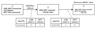
1) Is it possible to change the value of IINDPM by changing the resistance of the ILIM_HIZ pin during charging and input power switching?
    As background, we want to set IINDPM separately by hard switching because different voltages are input to VAC1 and VAC2 even when the SOC module is not activated.
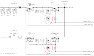
    Please give me your opinion if it is possible to hard-switch IINDPM from two different input sources in the circuit shown in the red box below.
    (I am assuming that if both inputs are present, IINDPM is to be set software).

2) If two different power supplies are used for input power and operated with a single input current limit, IINDPM is recommended to match which of the following conditions?
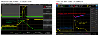
    VAC1: USB connection, 5V/2.4A
    VAC2: WPT power supply, 12V/1A
    Note that it is assumed that the ICO function is enabled during charging.

3) Is it correct that IINDPM is automatically adjusted to prevent the adapter from overloading even if the load status changes midway after the ICO function is enabled (EN_ICO = 1, ICO_STAT_1:0 = 2h)?
    If EN_ICO=1 is not enough for automatic adjustment, please let us know when to set FORCE_ICO =1 to prevent excessive current draw during load changes.

Regards,
Kagawa

  • Hi Kagawa,

    Regarding 1, ILIM_HIZ pin voltage is read at power up (after VBUS rises above VBUS_UVLO) and then not read again.  So it cannot be changed dynamically with the same power source.  If both sources are present, I don't think your schematic works.  Has this been tested?

    Regarding 2, when VACx turns off its xFETs and VACy turns on yFETs, ILIM_HIZ is read again because VBUS drops to zero briefly, even if a voltage is present at both VACx/y. I recommend sizing the ILIM_HIZ resistor divider for 5V/2.4A.  Then add a second resistor connected to a FET to ground.  The gate of that FET is tied to VBUS through a resistor divider that is sized so that the FET only turns on with 12V input source, not 5V.  The parallel combo of these 2 resistors reduces the equivalent bottom feedback resistance to set IINDPM = 1A.  

    Regarding 3, if enabled, ICO automatically reduces IINDPM when the input voltage droops to VINDPM.  The goal of ICO is prevent entering VINDPM regulation.  There is rarely a need to FORCE_ICO.

    Regards,

    Jeff

  • Hi Jeff-san,

    When both EN_ACDRV1 and EN_ACDRV2 are turned off and the VBUS voltage is set to 0V, I was able to switch IINDPM as intended with EN_ADC=0, but when EN_ADC=1 is set, IINDPM did not change from the value at input power-on.

    I would like to proceed with the evaluation with EN_ADC=0. Could you please tell me if there is a relationship between the ILIM_HIZ pin readout and the EN_ADC setting state, just in case?

    Regards,
    Kagawa

  • Hi Kagawa,

    Yes.  The charger repurposes one of the ADC channels to measure the ILIM_HIZ voltage at power up.  If EN_ADC=1, that cannot happen.  Glad to hear this works for you.

    Regards,

    Jeff 

  • Hi Jeff-san,

    1) Is it appropriate to execute FORCE_INDET=1 for the use of forced D+/D- detection under the following conditions?

        As background,
        VAC1: USB_DCP powered, 5V/2.4A
        VAC2: WPT powered, 12V/1A

        If they are connected simultaneously in this way and are being charged from the VAC2 side, when the power supply from VAC2 is stopped, USB charging will be done from VAC1, but IINDPM will not be greater than 1A. (The ILIM_HIZ pin has a resistor set to 2.4A.)

        In this condition, FORCE_INDET=1 will cause IINDPM to be greater than 1A, which is the intended maximum input current.
        Is this usage appropriate for the use of forced D+D- detection?
        Also, I would appreciate it if you could give me an example of a use case where FORCE_INDET=1 is required.

    2) Please let me know the specifications to be set for IINDPM under the following conditions.
        VAC1: USB_SDP power supply, 5V/500mA
        VAC2: WPT power supply, 12V/1A
        In this case, when I perform the following steps (1) to (3) to switch charging, IINDPM becomes 500mA when VAC2 is charged.


    I think that when charging from VAC2, the VBUS Stauts are judged as "Non-qualifide Adapter" and therefore IINDPM does not change from the previous value. Is this correct?

    3) I would like to set IINDPM = 1A whenever charging from VAC2. I would like to get your opinion on which of the following (1) or (2) is more appropriate as a timing to change the register setting software-wise.
    (1) When AC2_PRESENT_STAT =1, set IINDPM=1A
    (2) When VBUS Stauts is "Non-qualifide Adapter", set IINDPM = 1A.
    The concern is whether IINDPM=1A will be set when charging USB_DCP.

    Regards,
    Kagawa

  • Hi Kagawa,

    Regarding 1, D+/D- detect only works sources connected at VAC1.

    Regarding 2, yes.

    Regarding 3, that seems reasonable.

    Regards,

    Jeff 

  • Hi Jeff-san,

    Let me check again about the above query.

    1) Is it appropriate to execute FORCE_INDET=1 for the use of forced D+/D- detection under the following conditions?
         VAC1: USB_DCP powered, 5V/2.4A
         VAC2: WPT powered, 12V/1A

    3)  I would like to set IINDPM = 1A whenever charging from VAC2. Which of the following (1) or (2) would be the appropriate timing to change the register stting software-wise?
    (1) When AC2_PRESENT_STAT =1, set IINDPM=1A
    (2) When VBUS Stauts is "Non-qualifide Adapter", set IINDPM = 1A.

    Regards,
    Kagawa

  • Hi Kagawa,

    Regarding 1, D+/D- only works for VAC1.

    Regarding 3, either would work but I would wait for "non-qualified adapter".

    Regards,

    Jeff

  • Hi Jeff-san,

    I am considering connecting a USB type-c adapter supporting HVDCP with BQ25798 or BQ25790 to VAC1 and charging at 9V or 12V.
    In this case, we do not need an IC such as a CC port controller to detect HVDCP, and we can charge at 9V or 12V by setting the following register to 1 with this IC alone. Currently, we have set the registers as described on P.27 of the datasheet, but the charge is not higher than 5V.
    If the following settings are not sufficient, we would like to know if there is a way to set the input voltage from USB to 9V/12V when charging.

    Settings for HVDCP charging:
    - EN_HVDCP=1
    - EN_HVDCP=1
    - EN_12V=1
    - EN_9V=1

    Current register setting value:


    Regards,
    Kagawa

  • Hi Kagawa,

    Those settings are sufficient.  However, the dc/dc converter turns on before HVDCP starts.  If there is a large input current (usually > 500mA) flowing, the detection may not complete successfully.  Can you remove the SYS load and/or turn off charge and try again?

    Regards,

    Jeff

  • Hi Jeff-san,

    What is the percentage error between the value displayed in the IINDPM register and the threshold at which the input current is actually limited?
    As background, I set a resistor constant on the ILIM_HIZ pin of the BQ25798EVM so that IINDPM = 1600mA, but the IINDPM register displays 1580mA.
    I assume that this is due to an error in the resistor, but I have checked whether the current limit at VAC1 input is actually applied at 1580 mA by drawing current from the SYSTEM pin to the electronic load with this constant, and found that the limit is applied at 1490 mA in actual measurement, and the current cannot be drawn to 1580 mA indicated in the register. This is not the operation of IINDPM.
    Is this normal for IINDPM operation, or is it due to an error in reading the IC's internal ADC?

    State of connection of the evaluation board:


    IINDPM register display (IINDPM=1580mA)


    Resistance constant of ILIM_HIZ pin


    Regards,
    Kagawa


  • Hi Kagawa,

    The ILIM_HIZ pin voltage varies based on REGN voltage and resistor tolerance.  The ADC reads the ILIM_HIZ pin voltage at power up and sets the IINDPM register based on that.  We don't spec the ADC accuracy.   

    Below is the accuracy of the IINDPM regulation loop when set by the register.

    So the variation you see is due to the resistor accuracy (spec'd), REGN accuracy (spec'd if not in dropout), ADC accuracy (not spec'd) and IINDPM regulation loop accuracy (spec'd).

    Regards,

    Jeff

  • Hi Jeff-san,

    1. When the following procedure is followed, the intended IINDPM is set at the second input power connection.
    Can you please indicate the reason for this?
    In this use case, IINDPM does not increase from the previous value on the first insertion and removal. (The state of the red frame in the flow below)
    Is there a buffer inside the charger IC that remembers the previous IINDPM value based on the resistance value connected to ILIM_HIZ?


    2. When the following procedure is performed, the smaller of the register value or the ILIM_HIZ resistor may not be set to IINDPM. Is this behavior a specification?


    3. We would like to know if there is a way to set the VBUS Stauts to something other than "non-qualified adapter" when power is input to VAC2.
    The reason for this is that we are considering setting the input current limit to a fixed IINDPM without any operation by the host, rather than keeping the input current limit unchanged from the previous value.
    For example, are there any conditions under which VAC2 would recognize "Unknown Adapter - 3A"?

    Regards,
    Kagawa

  • Hi Kagawa,

    Regarding 1, I have repeated this flow.  The IC's ADC reads ILIM_HIZ voltage at each power up.  However, if ILIM register has previously clamped lower from ILIM_HIZ pin, it remembers and, as a safety feature, retains the lower setting.  To prevent this, the host can toggle EN_ILIM after the last read.  

    Regarding 2, the works as designed.  If EN_ILIM bit = 1, the ILIM_HIZ setting is used at each power up.

    Regarding 3, unfortunately, no.  Since D+/D- detection does not function with VAC2 input, the status will always required non-qualified adapter.

    Regards,

    Jeff

  • Hi Jeff-san,

    1. By which power source are the voltages (ACDRV1, ACDRV2) to turn on ACFET1-RBFET1 and ACFET2-RBFET2 boosted and generated?

    2. Currently, inrush current has been observed at the VAC1/VAC2 terminals as shown in the waveform below, and we are considering adjusting the gate resistance of the external FET and the constant of the capacitor to suppress the inrush current.
    We are considering the following circuit configuration, but would you please tell us how many μs the time constants of the gate resistor and capacitor can be tolerated as the specification of BQ25798?


    3. If the Schottky barrier diodes D104 and D103 in the circuit diagram are mounted according to the configuration in question 2,
    Can you please tell me the maximum current value that the ACDRV1 and ACDRV2 pins can draw?


    Regards,
    Kagawa

  • HI Kagawa,

    Regarding 1, VACx provides input power to the charge pump that provides the ACDRVx output.

    Regarding 2, the only timing constraint I can find is below:

    Regarding 3, I don't understand the purpose of those diodes. It is my understanding that ACDRVx doesn't sink current.  When ACDRx are turned off, a 6kohm pull down is applied to VBUS.

    Regards,

    Jeff

  • Hi Jeff-san,

    In Figure 9-4 on page 33 of the datasheet, when the gate terminals of ACFET1 and RBFET1 are switched after power is input to VAC1, there must be even a small current flow between ACDRV1 and ACFET1 and RBFET1 (same for VAC2 side).

    In this case, can you please tell us about the following?

    1) The current value that flows when the gate of the FET turns ON
    2) The maximum value of current drawn when the gate of the FET turns OFF


    Regards,
    Kagawa

  • Hi Kagawa,

    Regarding 1, I do not have that value.  It is in the 10s of uA.

    Regarding 2, as I mentioned above, when ACDRx are turned off, a 6kohm pull down is applied to VBUS.

    Regards,

    Jeff

  • Hi Jeff-san,

    Is it possible to present the internal circuit of the drive circuit part of ACDRVx?
    ACDRV is turning ACFET (Nch-MOS) on and off, so if 12V input is present, it should output more than 12V.
    Since conduction can be stopped even when VIN is present (can be set with a register), the ACDRV side is also performing the pull-in.
    My question is to understand the maximum drive capability (Sink/Source) of Gate.
    However, since there may be errors in recognizing the internal circuitry and operation, please explain the internal circuitry as we would like to have a common understanding.

    Regards,
    Kagawa

  • Hi Kagawa,

    The exact circuit details are proprietary so I cannot share.  ACDRV voltage should be V(REGN)+VBUS.  I will ask designer if we have the max source and sink for the ACDRVx pins.

    Regards,

    Jeff

  • HI Kagawa,

    The pulldown is ~100ohms. The pull up path to the charge pump output = V(REGN)~=5V + input is limited by about 25Kohm.

    Regards,

    Jeff

  • Hi Jeff-san,

    I believe an upper limit exists to keep the output of the charge pump constant.
    There may not be a limit for instantaneous current.
    I believe there is some design criteria in the schematic of the evaluation board (BQ25798EVM), because the diode is designed to be reserved in parallel with the gate resistor.
    I have determined that the output stop is the fastest when the diode is mounted in parallel with the gate resistor, if it is pulled down at 100 ohms.
    Is this understanding correct?

    As background to this question, we need to limit the rush current when connecting USB devices, and we need to limit the inrush current to the VBUS line passcons with ACFETs.
    We would like to address this issue by adjusting the time constant, so I am asking to know the recommended value.

    Regards,
    Kagawa

  • Hi Kagawa,

    The unpopulated diode in parallel with the ~300ohm resistor would speed up FET turn off if installed since it adds to the 100 ohm pull down resistor

    To limit inrush current, I recommend adding a gate to drain capacitor across Q1 or Q3.  As long as the RC time constant of the 25kohm and the total gate capacitance is less than 30ms, I don't see an issue.

    Regards,

    Jeff