This thread has been locked.

If you have a related question, please click the "Ask a related question" button in the top right corner. The newly created question will be automatically linked to this question.

TPS40211: PWM dimming

Part Number: TPS40211
Other Parts Discussed in Thread: ALLIGATOR, , TPS40210

Hi Team,

We would like to ask your help regarding our customer's inquiry below.

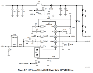
I went and built the circuit in Figure 8-7. I forgot to add the high-side resistor on the gate for the PWM input. I wanted a separate PWM input that customers can use. Should the high side resistor connect to BP or Vin?

I also forgot about the high side resistor and wondered on the "weird" behavior a bit. After figuring out the issue I connected a 3.3V battery(LiPo with low energy left) to + side of PWM and - to supply ground using alligator clips. I am using a benchtop power supply to power the thing and it behaves strangely. The power supply shows the circuit using only ~250mA at 12V, when I set the resistor to 0.5 ohm which means it should use at least that since it's a boost driver.

So I took a function generator and fed square waves to the PWM + input and connected - to supply ground again. The LED flashes under 95% duty cycle with 4V and 10KHz but at 100% the power supply shows it's using the expected >500mA.

Why do you suppose it is flashing? Also with the PWM input floating, with Vin of 5V it gets bright and pulls high amount of current, heating up the inductor significantly. The datasheet says that when the Vin is under 8V, BP is also under 8V.

I am thinking it's a various combination of quick and dirty alligator clips which picks up ambient noise and the Vin itself being dirty? It's a linear power supply but it's being powered by the inverter.

Regards,

Danilo

  • Hello Danilo,

    Thanks for reaching out to us via e2e.

    I am sorry, but I do not really understand your description.

    Can you please describe in a different way (maybe mark the items in a diagram):

    - the high-side resistor on the gate for the PWM input.

    - I wanted a separate PWM input that customers can use

    -  I connected a 3.3V battery(LiPo with low energy left) to + side of PWM

    Can you please use an oscilloscope and measure the switch node (starpoint between L1, Q1 and D1)?
    The voltage on the COMP pin would be very helpful as the second sinal.

    Please provide these oscilloscope screenshots for all use cases that you have described.

    Thanks and regards

    Harry

  • Hi Harry,

    Thank you for your response. Please see the feedback of our customer below.

    High side resistor: MOSFET inputs need the gate to be tied high(N-channel) with a high value resistor(not too high, say 100K) so when there's no signal, it does not float. I do not have that in my circuit.

    The chip datasheet has a PWM dimming circuit as part of the schematic. What I wanted was for a customer to use his own PWM device to dim the device as necessary. By tying the input of the PWM(thus gate of MOSFET) high, the default state would be LED equal to 100% duty cycle, if the customer chooses not to use PWM dimming.

    I am figuring some things out too as I found out the input is quite dirty thus the input for the function generator as well. I will clarify with pictures.

    Regards,

    Danilo

  • Hello Danilo,

    The voltage on the COMP pin will set the duty cycle.
    During normal operation, It shall range between about 1.3V (0% duty cycle) and1.4V (100% duty cycle).
    Disclaimer: These numbers are taken from a different device. I have not measured this myself on the TPS40211.
    Please measure it on your own board to find out what the exact voltage level will be.

    The idea that is shown in figure 8-7 is that the external FET shall pull down the COMP pin voltage to a level where the Duty cycle will go down to 0%.
    But it shall not pull it down too far, otherwise it would take too long for the capacitors of the compensation network to re-charge and to get back to the normal duty cycle.

    Therefore, the selection of these diodes is important.
    As I said, to be on the safe side, please measure the voltage on your own system.

    Regarding the frequency of the PWM signal: This should be selected as low as possible. Just that you do not see the flickering. Maybe a few hundred Hertz.
    Otherwise the compensation loop will have no chance to get back to a stable operation while the LEDs are on.

    That resistor R15 from the BP pin to the diodes/FET is important.
    It has to make sure that the cathode of the diodes has a higher voltage than the COMP pin, so that these diodes are blocking when the FET is off.
    So, please add a resistor of some 10K there.

    If it still does not work and you will need more detailed support, please provide oscilloscope screenshots, at least from the COMP pin and the switch node.

    Best regards
    Harry

  • Hi Harry,

    Here is the update from our customer.

    I have attached the pictures you asked for.
    TPS40211DGQ.zip

    Steps I have taken myself. The MOSFET is the TI recommended CSD19538Q3AT.
    -The Gate resistor was 24.9 Ohm, and I read in another thread to reduce the value so I have take it down to 3.6 Ohm. It didn't improve the situation, if anything it made it worse.
    -My goal is for the PWM input to work with Arduino and other microcontrollers. I have used Arduino, and also a function generator. Actually it's a cheap $50 one that you assemble as a kit. I was only able to get full 500mA brightness using that FG though.*
    -I thought of adding a 0.5-1uF capacitor from COMP pin to the gate as the recommendation in the thread. I have not done so yet.

    *When it's set to 3.7V I get full brightness. When I go above or below the voltage the current to the LED gets reduced. Actually below 3.7V it goes to the lowest brightness at 12V(the LED lights up dimly). At above 3.7V it's still bright but does down.

    The FG does not output 3.7V. It probably cannot supply enough current. It seems to be about 2V. The Arduino outputs a proper 5V PWM. The Arduino output is also cleaner but doesn't seem to make a difference. The default PWM frequency output for Arduino according to a search is 497Hz so not that high. FG is 1-10KHz.

    Below 100% duty cycle(actually it works to 97%) it has issues.

    Follow the names for the pictures attached.
    -Comp 240 means Arduino with 240/255 or 94.1% Duty Cycle. Comp means the voltage on the compensation pin
    -Comp 240-2 means second picture with 240/255. The spikes shown are random.
    -Comp 248 means 248/255 Duty Cycle
    -Comp 255 means 255/255 or 100%, meaning DC
    -Gate 240 means Gate of the PWM MOSFET with 240/255 Duty Cycle, Gate 248 means 248/255, and Gate 255 means Full, 100% Duty Cycle.

    Below 248/255 Duty Cycle the LED flashes. On my Fluke 87V, Comp pin shows anywhere from 1.392 to 1.398V with Duty Cycle at 248/255 or above. At below 248 Comp pin basically shows 0V.

    Sorry, I forgot to include the shots. I have tried the FG with low frequencies, and also 10KHz. Included are the pictures.

    The diode used is the recommended MMBD7000. The R15 value is 49.9KOhm.

    Arduino frequency is actually slightly under 1KHz. ~970Hz.

    Regards,

    Danilo

  • Hello Danilo,

    Thank you for the additional details.

    Today was a bank holiday for us and most people will also take Friday off.
    We will have a look at it and come back to you early next week.

    Best regards
    Harry

  • Hi Harry,

    We would like to request an update to our customer's feedback.

    Thank you!

    Regards,

    Danilo

  • Hi Danilo,

    Thanks for sending your waveforms and explaining you progress.
    To get a clear picture of this issue, please let me go one step back with this design.

    You mentioned you rebuild the circuit from figure 8.7 of the datasheet, which looks like this:

    Can you share the schematic of the customer board, so we can look at the actual design?
    We have an EVM for TPS40211 which has pin for the external PWM signal build in. Has customer used a sample EVM for their tests and did some modifications on the board, or are they working with their complete own design?

    You mentioned the PWM signal that comes from the external arduino that runs with approx. 1kHz.
    It might be interesting to look at the output voltage of the device itself. E.g. if there is strong oscillation due to system instability, it might become visible at the LEDs.
    This might occur when the PWM signal injected to the COMP pin interferes to strongly with the normal output regulation of the device.

    Best regards,
    Niklas

  • Hi Niklas,

    Please see the response of our customer below.

    It's my design. I should have took most of the advice from Figure 8-7 but it was a mix of Figure 8-7 and rest from webench. I kept the Rfb resistors to limit the voltage but after looking at other customer cases in TI support and doing some reading I should use another method to limit the output voltage.

    Further experiments:
    -Rfb taken out
    -D2 Zener and R24 taken out
    -Changed R11 to 100 Ohms
    -Tried 3.6 Ohm, 24.9 Ohm, and 62 Ohm for R2

    I did not use R13 in Figure 8-7, is that an issue?

    I am not going to attach the pictures of the output because there's nothing out of the ordinary. Output is ok at 100% duty cycle. Noise is 100mV or less for ~19V output. It shows more or less normal operation until about 250/255 duty cycle, but it starts showing significant fluctuation mirroring the gate and compensation graphs. Anything below that it flashes.

    Noticed another thing. Took my FG again. It's brightest(and LED current is expected at 500mA) when the PWM input is set at 2V with 100% duty cycle. Actually it should be 2.05V because at 100% duty cycle it's half of what I set at or 4.1V. If I go below that the brightness is pretty much equal to 0%. At above 4.1V, it gets steadily less brighter. When I set it to 10V(Arduino equivalent of 5V 100% duty cycle), I'm getting the same usage setting on my power supply.

    It seems to me there's a goldilocks zone on input PWM voltage to have the max brightness? Almost as if the MOSFET Q3 needs to turn on enough but fully saturated.

    Regards,

    Danilo

  • Hi Danilo,

    Thanks for the details.
    I will check through the schematic and give you some feedback earlier next week.
    Please note that there will be a holiday in Germany on Monday, so responses might get delayed.

    Sorry for this inconvenience.
    Best regards,
    Niklas

  • Hi Danilo,

    Sorry for the long delay.
    So customer build his own design based on webench and the datasheet.
    In general, it is always good to see the full power stage within the schematic, as it helps for checking the compensation, output capacitance and inductor, but if the design works fine for 100% operation time, I agree that we should focus on the PWM dimming circuit.

    R23 in the figure is for loop injection testing and therefore optional, R13 is directly connected to the feedback pin and adjust the reference voltage, therefore I would not assume it is optional.
    For additional resource in debugging the application, I would highly recommend the customer to get a sample of our TPS40210 EVM.
    https://www.ti.com/tool/TPS40211EVM-352
    T
    his EVM has been validation for proper functioning with dimming application, therefore it should be an even better reference than Webench.

    Best regards,
    Niklas

  • Hi Niklas,

    Please see the response of our customer below.

    Please ask the engineer why the Equation 34 says Iout (max) when the description for it says: "The peak-to-peak ripple is chosen to be 30% of the maximum input current". Based on the formula shouldn't it be saying "30% of the maximum output current"? Which is it?

    Regards,

    Danilo

  • Hi Danilo,

    The equations calculate based on a worst case scenario. For a Boost application, the input current is higher than the output current (Pout = Pin x efficiency).
    Therefore the equation uses the peak input current for the ripple current calculations, which can be transformed from the output current and the duty cycle.

    I am sorry if this equation causes confusion, as it is not explained in more detail.

    Best regards,
    Niklas

  • Hi Niklas,

    Please see the comment of our customer below.

    I suspected that. But equation 34 is this: Iripple(max) = 0.3 x (Ioutmax/1-Dmin)

    The description for equation 34 says "8.2.1.2.3 Inductor Selection

    The peak-to-peak ripple is chosen to be 30% of the maximum input current."

    If it is indeed using peak input current, shouldn't the equation be, Iripple(max) = 0.3 x (Iinmax/1-Dmin)?

    Regards,

    Danilo

  • Hi Danilo,

    Thanks for the feedback.
    Now I see where the misunderstanding comes from.
    The equation in indeed correct.
    You can either write the equation as:
    Iripple(max) = 0.3 x (Ioutmax/1-Dmin)
    or as:
    Iripple(max) = 0.3 x Iinmax
    because:
    Iinmax = Ioutmax/1-Dmin

    Best regards,
    Niklas

  • Hi Niklas,

    Here's a follow up inquiry of our customer.

    Could you please tell me why the example schematic in the datasheet and the EVAL board uses 10uH inductor and 15mOhm current sense resistor when the equation seems to show that it needs much higher values?

    If you follow through equations 32 then it becomes obvious that the minimum inductor size is much higher than 10uH. Vout of 35V and Vinmax of 14V with Ioutmax of 0.7 we get inductor values of 40uH or greater according to equations 32-35.

    Inductor
    Dmin = 35 - 14 + 0.5/(35 + 0.5) = 0.6056
    Dmax = 35 - 8 + 0.5/(35 + 0.5) = 0.7746
    Iripplemax = 0.3 x 0.7/(1-0.6056) = 0.5325A
    Lmin = 14/0.5325A x 0.6056 x 1/300KHz(EVAL board fsw) = 53uH

    Rsense
    If I follow through equations until equation 49, then I end up with Rsensemin value of 29mOhm, much higher than 15mOhm value.

    Is it different for LED drivers since the current limit is determined by the series resistor in conjunction with the feedback voltage and it essentially acts like a current limiter?

    It's obvious the biggest influencer for the final value of Inductor and current sense resistor is the Iout value, and since the Iout in the example used in the calculation is much higher(3x in fact), it increases the Iripplemax value by 3x, which reduces Lmin to 1/3rd, and that's why it uses 10uH Inductor and 15mOhm resistor, yet the LED drivers are using the same value despite having much less Iout.

    Regards,

    Danilo

  • Hi Niklas,

    Our customer would like to request an update to his inquiry.

    Thank you!

    Regards,

    Danilo

  • Hi Danilo,

    Thanks for reaching out to us via e2e.

    It is a bank holiday today. Please expect a response by Friday or Monday.

    Best regards,

    Feng Ji

  • Hi Niklas,

    I hope that you are now back from a holiday. We would like to ask for further support on this thread.

    Thank you!

    Regards,

    Danilo

  • Hi Danilo,

    I am very sorry for the long delay.

    Regarding the customer calcuations, they are completely correct. The datasheet would recommend a higher inductance for this application. I also checked with the quickstart calculator tool for TPS40211, which shows the same results.

    Unfortunately, I do not have any documentation which explains the inductor choice of the EVM in detail.
    EVMs are often designed to cover a large range of input, output and current variations to make them easier to modify by customers without large component replacement efforts. Because of this, some design are not fully optimized for the standard application.
    I would assume this is the case for this EVM as well.

    When designing their own application, I definitely recommend to use the values calculated by the datasheet and quickstart tool, to create the most optimized circuit for their application.

    Best regards,
    Niklas

  • Hi Niklas,

    Please see the follow up inquiry of our customer below

    The LED driver application circuit in Figure 8-7 uses similar values as well. 10uH Inductor and 15mOhm sense resistor. Maybe you can look into that too?

    I have another question. The sense resistor ground has to be on a different ground plane from IC ground and isns filter ground? It seems on the layout example IC ground is separate from isns filter + sense resistor ground while the EVM shows isns filter uses same ground as IC ground and sense resistor ground is on another plane.

    What is recommended? Shouldn't the sense resistor be on the same ground plane as the isns filter resistor + capacitor since it uses the sense resistor for calculating current limit? What about in respects to IC ground?

    Regards,

    Danilo

  • Hi Niklas,

    We would like to request an update to our customer concerns above.

    Thank you!

    Regards,

    Danilo

  • Hello Danilo A.,

    Sorry for the late response.

    The sense resistor is part of the high current output loop and therefore the GND connection will be noisy, especially if you are using PWM dimming.

    To have this noise somewhat decoupled from the IC and the filter caps, using a quiet analog GND for these sense signals is recommended. But make sure that the DC level of the noisy power GND and the analog GND is the same. I think the EVM gives a good example for a working layout.

    Best regards,
    Brigitte

  • Hi Brigitte,

    Our customer is waiting if he can get answer for the different-than-calculated values for example LED drivers. 

    Regards,

    Danilo

  • Hello Danilo,

    Sorry, but it seems there is an open question that I do not find. Would you please explain, what exactly your customer expects from us?

    Best regards,
    Brigitte

  • Hi Brigitte,

    Please see our customer's response below.

    Few messages back, I asked if the equations are correct. Then I said I noted the values are different from EVM AND the LED Driver example in the datasheet. The values should be way over 10uH for the inductor for example yet it uses 10uH.

    "The LED driver application circuit in Figure 8-7 uses similar values as well. 10uH Inductor and 15mOhm sense resistor. Maybe you can look into that too?"

    Regards,

    Danilo

  • Hi Danilo,

    The inductor is selected based on the assumption that "The peak-to-peak ripple is chosen to be 30% of the maximum input current."(eq.34). This is true for most application in CCM.

    But in the LED application, you may choose to operate the converter even in DCM. It has many benefits like fast transient and easy compensation. And due to the current is low, higher ripple current is acceptable. This means the peak-to-peak ripple is chosen to be 200%+ of the maximum input current. I suppose you can get a similar inductance and current sense resistor with much higher ripple factor.

    Best Regards,

    Feng Ji