This thread has been locked.

If you have a related question, please click the "Ask a related question" button in the top right corner. The newly created question will be automatically linked to this question.

UCD9090A: UCD9090a

Part Number: UCD9090A
Other Parts Discussed in Thread: UCD9090

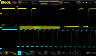
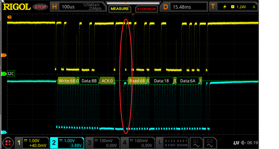
Using our I2C adapter inside our Xilinx FPGA XIIC to communicate to the UCD9090A over the PMBus, and using a Salae logic analyser to capture the waveform below, we are reading command 0x8B, the device address is 0x68.  Every so often, like 5% of the time the device is not ACKing its address.  From this snapshot, it looks like a valid I2C transaction with a NAK instead of an ACK from the UCD9090.  Any idea why this would be happening?


  • Hi

    Does the host support clock stretching? 

    Please use scope to capture both good and bad transaction. Do not use logic analyzer which can not disclose the details. 

    Regards

    Yihe

  • I am told by the FPGA engineer that the host the xilinx xiic does support clock streching but I have also asked them to double check with Xilinx.  Here this is clearly not a clock streching issue as the clock is not being held low.  Sorry about swapping the probes(colors) between the 2 captures

  • Hi

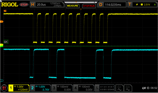
    is this from UCD side or FPGA side? It does not look like a complete transaction and 2nd wave show a NACK on the write.

    what happen before this? Is there a timeout(SCL low more than 35ms)?

    Regards

    Yihe

  • Hi Yihe,

    I don't understand your 1st question, the bus is between the FPGA and the UCD and we are capturing scope screenshots between the 2 devices.  Correct this is what we don't understand, why sometimes the device doesn't want to ACK and we see the NAK.  Before we were just reading an input file using the linux shell command we basically keep doing a "cat in10_input" over and over and sometimes we just get this failure.  Keep in mind that this is done by hand using the shell so very slow device access.  So before it fails we have a bunch of successful reads.

  • Hi

    My first question is whether the waveform measurement is from UCD side or FPGA side. 

    Could you provide a log to show all the I2C transaction until fail and provide the waveform before the NACK case so that we can see what exactly happen before?

    Regards

    Yihe

  • Hi ,

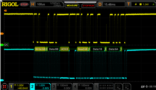
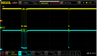
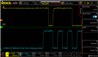
    We have a Xilinx XIIC (I2C) device connected to a level translator (1.8V to 3.3V to a 2 * 5  pin connector we use for the TI dongle, which is disconnected, the connector is used for the SDA and SCL clock probes and then straight to the UCD 9090A.  I have added 3 screenshots, one that shows a good transaction followed by a failure, and both good and bad transactions zoomed in.

  • HI

    Is this a repeated-start or stop-start?

    UCD does not support stop-start for read operation.

    Regards

    Yihe

  • Hi Yihe,

    It is a repeated-start. 

    Regards,

    JP

  • Hi

    But the rising edge of the SDA is also the same on the falling edge of the SCL. That's why it is important to know the capture is from UCD side or not.

    Maybe you can compare the good case and bad case on this repeated start .

    What's the pull-up resistor used on the SCl/SDA?

    Regards

    Yihe

  • Hi Yihe,

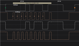
    The XIIC allows us to move the SDA edge changes in the middle of the low clock, which we have tried with no changes in the result, it didn't fix our problem, for instance, we had it in the middle of the low clock, it still failed once in a while.  Please note that the failure (NACK) happens when we write the device address, so there are no repeated start in the failed transaction , it is only one byte with address 0x68, W the UCD doesn't see it and doesn't assert the ACK.  the resistors on both signals, SDA and SCL are 2.4K.  One difference we noticed is that the dongle has a bit of a delay before it issues the 9th clock for the ACK as shown below, here we used address 0x0B for a device that doesn't exist on the bus to make sure the delay was added by the dongle.

    Regards,

    JP

  • Hi

    ADDRESS ACK is handling by IC and if it is NACK, it means that the state machine was not in the right spot due to some past bad transactions. 

    we need see the transaction before the NACK.

    Please share your new waveform with SDA rising at the middle of SCL low.

    are you using dongle to test? 

    Regards

    Yihe

  • Hi Yihe,

    We are seeing this problem on each transaction before a failure,  so you are %100 right the previous transaction is messing up the state machine, here the stop bit identified with the reddish square the clock should stay high, but it is transitioning for some unknown reason back to 0 at around the same time as the data is going high (reddish square).  This is with the XIIC device, we never see this with the dongle.  With an I2C clock problem, it is not easy to put the blame on the master or slave device when the clock goes low,  but because it never happens with your dongle,  I am going to blame the XIIC or its device driver, so we are going to work on this now.   Thanks Yihe.  If you don't mind let's keep this open, I will keep you posted.

  • Hi

    Please update us on this.

    Regards

    Yihe