A related question is a question created from another question. When the related question is created, it will be automatically linked to the original question.
If you have a related question, please click the "Ask a related question" button in the top right corner. The newly created question will be automatically linked to this question.
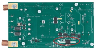
UCC28951: What is the evaluation board UCC27714EVM-551?
Any of our EVM's work best as a real-time simulator. They are best used to understand how the device(s) are working when everything is perfect. This can be used as a baseline for your own design if you try to design for a different output voltage or power level. The EVM guide is the best way to prepare for how to use the EVM.
CS is pulled up to VREF typically via a 1k resistor. This is the output of a current sense transformer:
ADEL and ADELEF are used to optimize the efficiency of the design by adjusting the dead time. I would have to check with the designer of the EVM to see why this wasn't necessary to set.
The CS pins in the EVM design is not connected to VREF. A resistor divider from the reference is connected to ADEL and ADELF to use a fixed delay approach as described in application note slua560d.
The fixed delay approach is the most popular design using the PSFB. It is easy to setup and is quite efficient with ZVS. The adaptive delay approach is used by some to reduce body diode conduction on the primary of the H Bridge. This efficiency improvement from removing the body diode conduction is marginal compared to what you achieved for ZVS. To setup the timing is also a lot of trial an error. For these reasons most designer choose the fixed delay approach described in application note slua560d.
The adaptive delay technique which would would have resistor dividers from CS to ADEL and ADELEF. If you decide to use this technique I believe there is information in the data sheet on how to use adaptive delay. Also you would just have to unpopulated the resistors between ADELF and ADEL to VREF. Then you would populate the resistors between CS and ADEL AND ADELEF.
I looked at the EVM and it looks like the designer tied ADEL and ADELEF to ground through a 0 ohm resistor. Setting the voltage at these pins to zero is an option.
In the equations TABSET, TCDSET and TEFSET you just need to set CS to 0 V in the equations to calculate the delays. To select the timing resistors you just need to algebraically solve for RAB, RCD, and REF.
The other option you have is to set the delay timing by setting the ADEL and ADELEF with a voltage with resistor dividers from Vref to these pins as described in application note slua560d.
The UCC28951 is a very versatile controller. You can design it for fixed delay or adaptive delay. You can adjust the voltages at ADEL and ADELEF with a voltage divider off of Vref, or the CS to get different timing behaviors. As you discovered you, can short the ADEL and ADELEF pins to ground if the designer choose.
That cutout under the digital isolator separates the primary from the secondary. It was done to meet creepage and clearance requirements.
In regards to the input voltage the transformer was designed for a 370 V input. So you will run into duty cycle and load regulation issues if you go below the minimum input range of the EVM.
If you need to design for a lower input range the transformer in the EVM will not work. You would need a new transformer with a different turns ratio and magnetizing inductances. Application note slua560d has a section on how to calculate these values ;as well as, RMS currents. You can then use these values to have a new transformer designed for you application.
Regarding the U4 isolator, the part number in the schematic and the part number in List of Materials in the user guide are different, which is correct?
More than likely when the board was designed one opto was used. Do to the part shortages the opto was swapped out. So both opto isolators should work in the desing.
They protect the DRIVE pins of the UCC287714 from negative voltages in regards to the FET source pins they are driving.
In some cases the parasitic inductance in traces can ring with parasitic capacitances. To protect the driver pin a shottky diode is added from the drive pin to the source pin of the FET at the gate driver integrated circuit.