I have a customer who would like to use one of our eGaN HEMTs as the external switching elements for the LM5116 IC controller.
The circuit that I would recommend to them looks like the following (shown just for the power train elements):
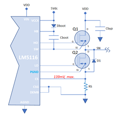
The transistors Q1 and Q2 are the EPC Space FBG10N05A. This is a 100V/5A eGaN HEMT, and its data sheet may be found here: https://epc.space/documents/datasheets/FBG10N05A-datasheet.pdf. The transistor package has four pins, gate/drain/source along with a "source sense" pin. The source sense pin is at the same potential as the source connection directly on the transistor's die. The source sense pin is a "clean" connection to the transistor's source connection at the die, bypassing common source inductance (CSI)and resistance (CSR). This allows the gate drive loop current to be decoupled from the drain-source current, and the result is a gate drive signal that is very clean, without perturbations caused by the high-frequency drain current due to CSI and CSR.
To get the maximum benefit from the source sense pin (SS) it is necessary to connect the return of the gate driver to that pin. For the high-side driver and transistor (Q1), this is possible because the SW pin on the LM5116 IC is the return for the high side gate driver (output at HO). The low-side situation is complicated because the low-side gate driver (output a LO) return is common with the PGND pin on the IC. In order to achieve the proper gte drive loop situation, the PGND pin must be connected to the SS on the low-side transistor, Q2. However, in the LM5116 data sheet there is the recommendation to "Connect to PGND and AGND through the exposed pad ground connection under the LM5116". This means that the situation in the example circuit, above is not possible because the voltage at the PGND pin would be at worst-case peak over 139mV:

With a peak voltage across RS determined by the inductor ramp and the response time from the current sense comparator to the gate driver output.
My question is can the PGND and AGND pins be at different potentials, or are these nodes at the same potential on the die, and MUST be connected together on the application PCB??? As you can see, the maximum voltage offset between PGND and AGND (the actual system "ground" return) would be 150mV, maximum. If AGND and PGND are indeed separate nodes on the die, can these two return signals have the differential potential of less than 150mV between them, with the PGND pin being at the higher potential?
Any help that you can provide me, or insights regarding the LM5116 would be greatly appreciated.
Best regards...
Tony Marini
Power Technologist
EPC Space, LLC
www.epc.space