- Ask a related questionWhat is a related question?A related question is a question created from another question. When the related question is created, it will be automatically linked to the original question.
Hi Team,
Greetings for the day.
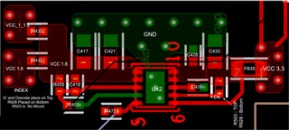
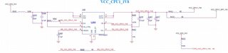
We are using the TPS7A9201 LDO in our Layout Board file. I had attached the images of the Board file and Schematics. Please review the layout and share your feedback with us.
The PCB we are using is of 12 Layers:
IC and discrete parts - Place on Bottom
Layers 2,4,9 and 11 are Ground
Thanks and regards
- Teja.