This thread has been locked.

If you have a related question, please click the "Ask a related question" button in the top right corner. The newly created question will be automatically linked to this question.

LM5157: Instability issues

Part Number: LM5157

Hi all, 

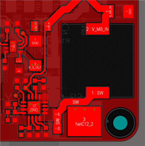
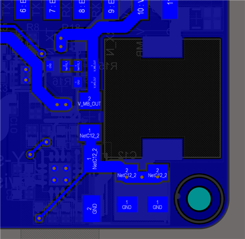
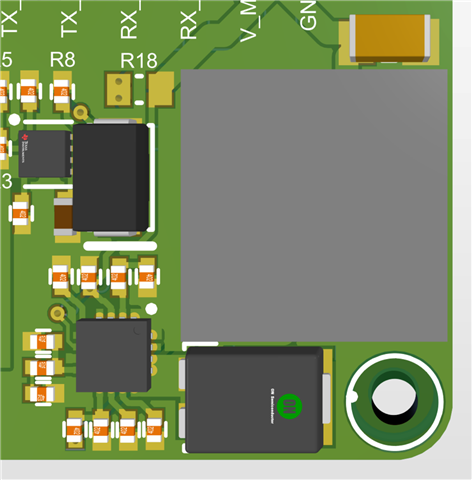
I am using the LM5157 in a 12V/24V, 2A design. Below is the schematic:

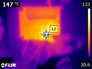
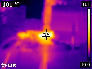
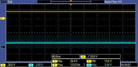
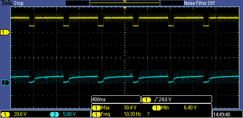
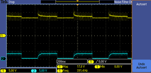
At I_LOAD above 1.5A, the design becomes unstable in about 90 sec: the output starts glitching, before dropping to ~12V. The output and SS waveforms after the instability event are attached below:

Double checking with WEBENCH, I changed R9 to the recommended value of 1K. This improved the situation, however it still became unstable after 5 min. Changing C17 to 10nF (recommended value) worsened the performance and it became unstable after 3 min.

I am not sure of the consumption profile of the load and doubt that it will draw 1.5A or even 2A constantly, however I would like to improve the robustness of the design.

Any advice would be much appreciated.

Regards,

Boris

  • Hello Boris,

    Thanks for reaching out to us via e2e.

    The simple answer is: You will need to select a different inductor.

    The inductor needs to be able to handle the peak current, so do not calculate with the average current.
    When the inductor heats up, the inductance value will go down below the nominal value.
    The fact that the problem comes in after a while proves that this is not a systematic failure but some kind of thermal issue.
    Also, the higher the switching frequency the more it will heat up. Is 1 MHz really necessary?

    When the peak current reaches the saturation current, it has already lost about 30% of the inductance. (only 3.3uH instead of 4.7uH).
    With the reduced inductance value, the converter will go into overcurrent (hiccup mode) and ultimately shut down.
    See chapter 8.3.11 in the datasheet.

    When choosing a different inductor, verify if it can actually handle the frequency.
    The degradation of the inductance will not only depend on the current and the temperature but also on the frequency.

    To make the feedback loop / compensation more stable, choose 4.7K for R9 and increase C17 to 22 nF

    The quickstart Calculator which you can download from here www.ti.com/.../snvr511
    will help you to understand the influence of the inductor and allows you to experiment with different compensation components.
    Please keep in mind that the parasitics of the actual hardware will have an influence on the compensation,
    therefore these calculated values may not really fit.

    Best regards
    Harry

  • Hi Harry,

    Thank you for your comprehensive reply.

    The inductor used is CDRH105RNP-4R7NC and has a saturation current of 6.4A. From my calculations, for Iload = 2A, ILpeak should be around 5.4A. Testing at Iload = 1.5A, the ILpeak should be around 4.2A. Do you think the margin is not sufficient?

    As for the temperature, the inductor is physally close to the LT5157 and D2 and during the test its temperature does exceed the recommended 100C. However, I also did some tests with the inductor suspended in air. The converter still fails, and the inductor temperature was around 70C.

    The MODE pin is grounded via a 0-ohm resistor, so hickup mode is disabled. Could the waveforms be related to thermal shutdown?

    So far the best results I have were with R9 = 1k, C17 = 10n, Fsw = 500kHz, where the converter was stable for about 10 mins. I tested earlier with the original compensation values (same as the screenshot) and Fsw = 500kHz, and did not find the results very different, i.e both times it failed. So I would assume the main culprit is the compensation...

    Now you are recommending values that are close to the original ones that have performed worse. Is it possible that a suboptimal compensation circuit causes increased heat dissipation and the failure after a while? Do you have any design guides for this? (This is an area I am unfamiliar with.)

    In the next revision I will change the inductor to a higher current/temperature part and will improve the layout in addition.

    Kind regards,
    Boris

  • Hello Boris,

    There is no rule of thumb for a margin.
    All inductors have a certain profile how the inductance changes with current and temperature.

    At high temperatures, the inductor you selected first show a slow decline, but at about 4.5A there is a steep drop.
    A lower inductance results in an even higher peak current, which is a vicious circle.

    I am sorry, I did not verify what the mode pin actually controls in case of this particular part.
    In case of other devices, disabling the hiccup mode means that it turns off for longer and does not preiodically try to start-up again.

    I do not really believe that this would be a thermal shutdown, as the die would need to reach a temperature of 175°C.

    Anyway, you can use a coolant spray, to cool down particular parts of the circuitry individually to see which one of them would make a difference.

    I had recommended using the same "old" resistor, but a much higher capacitor.
    Again, please use the Quickstart Calculator to experiment with the settings for the compensation network:
    www.ti.com/.../snvr511

    In reality there are parasitics on the board which will influence the compensation, so that these calculated values will only be an estimate.
    So, your experiments can result in different optimizations.
    Still, I would try increasing that capacitor.

    In general, the compensation should only be important in case of a change of the load or the supply voltage which needs to be compensated for.
    The compensation will then determine if the reaction on this change will be fast (maybe with ringing) or slow.
    If there are no such changes, the compensation should not be critical (unless the system is that close to the edge that a thermal influence will ultimately make it unstable).

    Before creating a new board/layout I would suggest that you first experiment with different inductors on the existing design.
    Mounting the inductor vertically and placing a wire between the current sense resistor and the inductor will not have too much effect on the performance.

    In fact, for experimental use, you can even connect the inductor with two wires to thermally de-couple it from the rest of the board.

    Best regards
    Harry

  • Hi Harry,

    From your reply, it sounds like the compensation can be eliminated as the potential cause as the load does not change during testing. When describing the results that follow, the original values in the schematic were used. These roughly align with the recommendations from your first reply.

    To begin with, I tried forced air cooling on the whole board. This made the design stable, however it is not something I can do due to the intended application.

    In some previous tests I decoupled the inductor thermally from the rest of the board. This still resulted in instability.

    I also experimented with some larger inductors with plenty of margin (7443251000 and SRP1050WA-120M). Both did not produce different results.

    Finally, I tried heatsinking the diode and the IC. Both have resulted in instability, with a slight difference:
    - when heatsinking the diode, the output voltage begins oscillating.
    - when heatsinking the IC, the output voltage oscillates for a bit, then the IC stops switching and the output drops to the input voltage. The diode goes into thermal runaway with temperatures above 250C.

    I am afraid I find myself in a dead end here: In the case of the diode heatsink, the inductor, diode and IC are well within their operating temperatures, approx. 100C, 110C and 140C and even with the smaller 10uH inductor (7443251000), there should be a sufficient margin for the inductance drop.

    Any further help that you could provide would be appreciated.

    Regards,
    Boris

  • Hi Boris,

    Thanks for the update.

    Today is a public holiday in Germany, therefore responses may get delayed.
    I will look into your question and get back to you by the middle of this week.

    Thanks for your patience.

    Best regards,
    Niklas

  • Hi Boris,

    Sorry for the long delay.
    From the history of this thread, I agree that it does not look like a compensation issue.
    If the selected component align with the quickstart calculator results, this should not be a part selection problem.

    As high temperature seems to have a strong impact on the system behavior, I would try to focus on the layout.
    You already talked about the placement of the inductor and the diode, but could you share a picture of the power stage layout?
    We may find some possible optimization to improve the thermal behavior.

    Another resource I would take into account is the LM5157 EVM, which has different voltage ratings, but similar current requirements:
    https://www.ti.com/tool/LM5157EVM-BST
    This design does not seem to heat up to more than 50C at full load, so if your design heats up above 100C, there might be stronger leakages.

    Best regards,
    Niklas

  • Hi Niklas,

    Monday was a holiday here in Norway also, so no worries.

    I am attaching the layout. Most of the components are on the top side, with the output capacitors and some filtering on the bottom. I agree it is not the best layout in terms of heat dissipation, but there are some size constraints to the design.

    I am also attaching some thermal images (top view of the inductor and LM5157, side view of the diode) and the output trace when the instability occurs. In this case there is a heatsink placed on top of the diode. Without the heatsink, the frequency would increase gradually until the switching shuts off completely, the output goes down to Vin, and the diode goes into thermal runaway and reaches 250+ degrees.

    Regards,

    Boris

  • Hi Boris,

    Thanks for sending the layout pictures.
    Here are the comment I have on the layout:

    - Current path traces of the power stage are a bit narrow (especially the wire to the inductor)
    It is recommended to connect the power stage components with copper polygons, instead of wire traces
    - Larger GND areas
    The GND area below the diode is rather small and connected the the other layers with only a few vias
    Please make sure the GND areas are as large as possible
    - Full circuit very close the PCB edge
    This will limit the heat sink by a large amount.
    If possible, please move the hot components a bit more into the center of the board, so there is more copper in more directions.

    Best regards,
    Niklas

  • Hi Niklas,

    Thank you for your feedback. I will improve the layout accordingly.

    Do you have any idea what is causing this behaviour? As you can see from the thermal images, the IC and diode are within their operating temperatures.

    Regards,

    Boris

  • Hi Boris, 

    Thanks for the feedback. Do you by chance have an EVM that you can try out? How does the CS pin, FB and SS look like? Has any component been replaced in the meanwhile (like the diode or the inductor or the IC)? What happens if you remove the zener at the output (its tolerance seems ok, but I would still like to try to remove it)?  We might need to take a further look at this and come back to you. 

    Kind regards,
    EM

  • Hi EM,

    Thank you for following up on this.

    No, I do not have the EVM. The only component change has been Css (C15) to 1uF. Removing the Zener has no effect.

    As for the measurement, the LM5157 does not have a CS pin, so I am not sure which one you are referring to. When I try to probe the FB pin, the output drops to 20V. I am attaching the output (channel 1) and FB/SS (channel 2) traces.

    To summarise the behaviour, when the output begins to flicker, the frequency of the flickering increases until the output drops to Vin and the diode goes into thermal runaway (250C+). If the diode has a heatsink, then the flicker frequency remains the same for a constant load. Increasing the load causes the flicker frequency to increase, but still remains stable.

    I hope this information is of use.

    Kind regards,
    Boris

    Output and FBOutput and SS

  • Hi Boris,

    Thanks for reaching out to us via e2e.

    It is a bank holiday today. Please expect a response by Friday or Monday.

    Best regards,

    Feng Ji

  • Hi Feng,

    Thank you for escalating this. Could you let me know what the status of the case is?

    Regards,

    Boris

  • Hi Boris,

    based on your thermal images it looks like the Diode is heating up much more then expected.

    Base on my math the RMS in the diode (Vin:12V / Vout:24V Iload: 2A) should be ~ 3A. With a voltage drop of 0.3V this would give a loss of ~ 1W and the temp. increase with the land pattern used should be less but increasing the copper area for the diode to spread the heat would be good as well.

    Can you please confirm that the large heating is coming form the Diode only. I am not sure about the thermal image and the component references.

    It would be good if you can measure the inductor current to ensure this is behaving as expected and no saturation effects are happening.

    Best regards,

     Stefan