This thread has been locked.

If you have a related question, please click the "Ask a related question" button in the top right corner. The newly created question will be automatically linked to this question.

UCC21710-Q1: Different Dead time in input and output

Part Number: UCC21710-Q1

Hi Team,

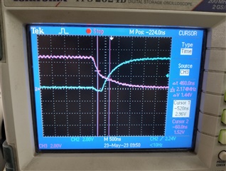
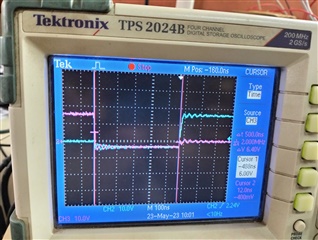
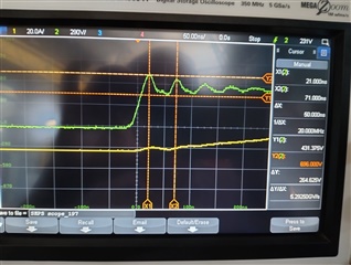
I am using UCC21710-Q1 driver IC for SiC MOSFET (C3M0040120D). 50kHz signal is generated with 160ns dead time using DSP board. The output from the DSP card is given below with 160ns dead-time.

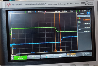
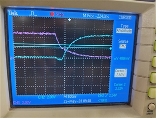
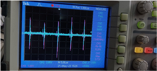
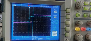
Same signal is given to input to the Driver board through FRC cable and the output of the driver is given below 

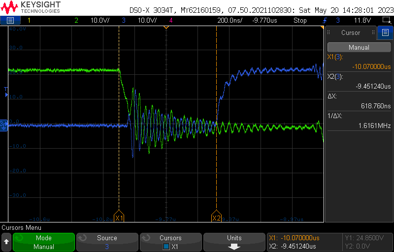
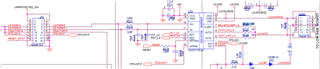
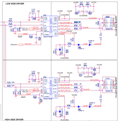
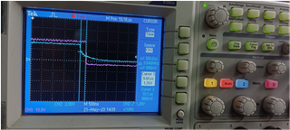
I have observed that there is Dead-time difference of 350ns. Can you please suggest, why this extra dead-time is adding to gate pulses. I have added RC (R=120R and C=56pF) filter at the input of the driver IC as per the datasheet. The driver circuit is given below for your reference 


Thanks in advance for your inputs. 

Regards

Umamaheswararao

  • Hi,

    Just to clarify, are you using more than one gate driver device in your system? What is the IN- signal? Please let me know. 

    Thanks,

    Nancy

  • Hi,

    Thank you for the reply. Yes, I am using two gate drivers, one for Top-switch (Higher-side) and second one is for Bottom switch (Lower-side). The schematic is given below

    IN+ and IN- signals are square wave pulses with dead time 160ns (Fig can be available in my previous post)

    Please help in this regards.

    Thanks

    Umamaheswararo

  • Hi,

    Thanks for the clarification. There are two built-in delays we would expect: the input filter deglitch time and the propagation delay. However, these would cumulatively add about 150ns of latency. What could cause delays of this magnitude is an unintended OC fault being triggered. Could you probe the OC pin to see if this is the case?

    Thanks,

    Nancy

  • Hi,

    Thank you for the reply. I have taken the OC pin signal for with and without MOSFET connections. I also observed that there is delay in same input (LS_in or HS_in) and output signals (LS_out or HS_out) of the driver. I have added my observations and figures below

    Driver Dead-time analysis

    1. OC signal without MOSFET connection (in CON1, PIN-1 and PIN-2 shorted)


    CH2: OC pin of UT3

    CH3: OC pin of UT2

    1. OC signal with MOSFET connection

    CH2: OC pin of UT3

    CH3: OC pin of UT2

     I also observed that there is a delay in the input and output of the same signal and are given below


    1. LS-PWM_IN Input ( at JT1) and output of the driver (at CON1) without connecting MOSFET


    Observed that dead-time is difference of ON-time delay and OFF-time delay i.e., 760ns

    1. HS-PWM_IN Input ( at JT1) and output of the driver (at CON1) without connecting MOSFET

    Same delay for HS_PWM signal.

     Thanks in advance for your inputs. 

    Thanks,

    Umamaheswararao

  • Hi,

    I see. Thanks for the additional information. Can you redo the deadtime measurements but measure the output close to the gate driver? This will give us more accuracy. 

    Thanks,

    Nancy

  • Hi,

    Thank you for your inputs. I have solved the dead-time issue. I found that ground connection is missing in the control card. The input and output waveforms are given below

    INPUT pulses 
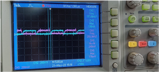
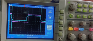
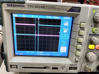
Input pulses with dead-time 340ns

    OUT_pulses 
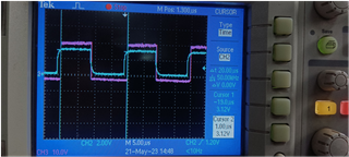
OUTPUT pulses with dead-time 440ns
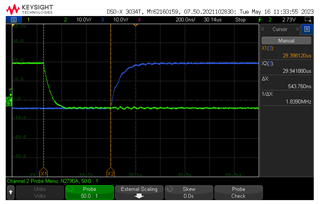
    If I am not wrong this 100ns is the propagation delay of IC. 

    Thanks

    Umamaheswararo 

  • Hi Umamaheswararao,

    For more accurate measurements you should place the cursors at the threshold voltages of the IN+ which would be 1.85V going HIGH and 1.52V going LOW when VCC1 = 3.3V.

    Nevertheless these results look to be what is expected from the gate driver. There will be slight differences in deadtime due to the propagation delay mismatches and also influenced by where you're placing cursors for measurement.

    Best regards,

    Andy Robles

  • Hi Andy,

    Thank you for your reply. I have measured the input and output close to the gate driver IC. The waveforms are given

    As per your calculations (for Vcc 3.3V),  here, Vcc is 5V and I placed the cursers at the threshold voltages of the IN+ which would be 2.8V going HIGH and 2.32V going LOW, same is given below


    The dead-time around 460ns. But my input signal from the DSP is 340ns, extra 120ns is adding.

    1)Is this extra dead-time is because of RC filter? can you please clarify this. How to design the RC filter for this IC, 

    2)Can I connect filter capacitor across IN+ (pin10) and IN-(pin11) to limit the noise, if yes, what value is best? 

    the out signal at the IC pins are given below (without MOSFET)

    The dead-time around 500ns. around 40ns dead is adding by IC maybe because of propagation delay. 

    When I connect actual MOSFET leg, the dead time is same but oscillations are produced. same waveform (Vgs of two mosfets) is given below 


    These oscillations are more when I load (9000W) the converter. the corresponding Vgs signals are given below

    3) Can you please tell me what parameters effecting this oscillations, Is this because of Ron and Roff?,

    I have selected same (10 Ohms) for Ron and Roff.

    4)What is the best combination of Ron and Roff. 

    Thanks in advance for your inputs.

    Regards

    Umamaheswaraaro


  • Hi,

    In UT3, the pins APWM and AIN are not used. what is the recommendation connections for this pins if we don't use.  

    Thanks and Regards

    Umamaheswararao

  • Hi Umamaheswararao,

    The dead-time around 460ns. But my input signal from the DSP is 340ns, extra 120ns is adding.

    1)Is this extra dead-time is because of RC filter? can you please clarify this. How to design the RC filter for this IC, 

    You are correct. Looking at the waveforms you can see your DSP changing states from ON to OFF state in one signal and OFF to ON state in the other signal with 340ns time difference, but from the thresholds(2.8V and 2.3V) there's about 460ns dead-time. This is due to the RC input to the gate driver. The RC filter increases the input signal robustness under noisy conditions. The added delay due to the RC must be included in your analysis to make sure you have the targeted dead-time per your requirements.

    2)Can I connect filter capacitor across IN+ (pin10) and IN-(pin11) to limit the noise, if yes, what value is best?

    RC filters at the input pins of the gate driver is common practice to increase input signal robustness under noisy conditions. Noise can be reduced by good layout practices and RC filters are just an additional protection. The smaller the time constant of the RC the faster slew rates you'll have on the input signals, but also less effectiveness of the RC against noise. Typical values for the R we see are 10Ω-100Ω and for the capacitor 10pF-330pF.

    3) Can you please tell me what parameters effecting this oscillations, Is this because of Ron and Roff?,

    I have selected same (10 Ohms) for Ron and Roff.

    4)What is the best combination of Ron and Roff. 

    One of the factors for gate oscillations is the parasitic inductance in your gate loop. The parasitic inductance can be reduced in the layout by minimizing the physical distance of the gate driver output to the GATE of the MOSFET, using wide traces for the overall gate loop (driver output and return path). Parasitic inductance can also de damped by increasing the gate resistor value, but this can also have negative impacts on your switching speed. A ferrite bead can also be used in the gate path to reduce the high frequency noise. You can refer to the below links for further information on gate ringing mitigation methods:

    In UT3, the pins APWM and AIN are not used. what is the recommendation connections for this pins if we don't use.  

    When not using AIN-to-APWM feature the AIN pin should be shorted to COM and APWM pin in the primary should be left OPEN.

    Best regards,

    Andy Robles

  • Hi Andy

    Andy Robles said:

              Typical values for the R we see are 10Ω-100Ω and for the capacitor 10pF-330pF.

    As per your suggestions, I have added RC filter (R=120Ω, C=220PF) . I want to know one thing here, this RC filter is connected after the voltage buffer (74AC573) and the current rating of this IC is +/- 25mA. This voltage buffer IC used to change 3.3V to 5V. 

    1. Now, during ON time, voltage applied across the RC filter is 5V, at the time of starting this demands (5V/120Ω) 41mA. This current is more than the output rating of the IC. If I use below 100Ω, it may draw more current. How to choose exact combination of R and C? How this RC filter effect on buffer ICs. 

    Andy Robles said:

    A ferrite bead can also be used in the gate path to reduce the high frequency noise.

    Thank you for the suggestion, I have used 200Ω, 100MHz ferrite bead with external gate resistor (15Ω). Now, gate signals noise is reduced. 

    But, Vgs oscillations are 20Mhz during ON and OFF and same are observed in primary voltage of the transformer and the corresponding waveform is given below

    Thank you for your inputs

    Regards

    Umamaheswararao

  • Hi Umamaheswararao,

    1. Now, during ON time, voltage applied across the RC filter is 5V, at the time of starting this demands (5V/120Ω) 41mA. This current is more than the output rating of the IC. If I use below 100Ω, it may draw more current. How to choose exact combination of R and C? How this RC filter effect on buffer ICs. 

    The resistor of the RC filter is purely for filtering purposes. It will not add significant current draw to the buffer. The input IN+ pin of the gate driver has an internal pull down which connects in series with the 120ohms. The value of the internal pull down is 55kΩ typical. With total resistance being 55.12kΩ the current draw would be 5V/55.12kΩ=~91uA.

    But, Vgs oscillations are 20Mhz during ON and OFF and same are observed in primary voltage of the transformer and the corresponding waveform is given below

    Seems these oscillation are typical in these high power application. The main power loop path ringing is also affected by the parasitic inductance in the design. Best way to try to reduce this is by physically reducing the power loop path in the system.

    Best regards,

    Andy Robles