This thread has been locked.

If you have a related question, please click the "Ask a related question" button in the top right corner. The newly created question will be automatically linked to this question.

TPS6594-Q1: Update to Forced-PWM mode in in 3-Phase Configuration

Part Number: TPS6594-Q1

Hi,

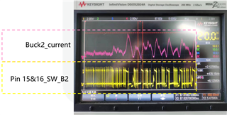
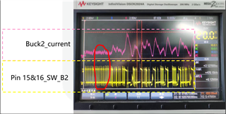
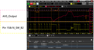
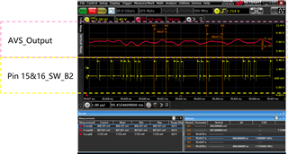
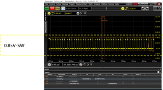
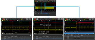
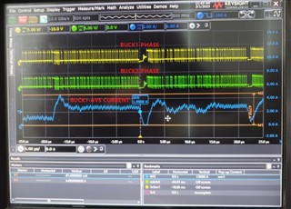
We used 1212 and 1111 power solution for TDA4 soc. The AVS output of 1212 is PFM mode after boot successfully.

Now we wanted to change AVS to PWM mode, and rewrote bit1/bit2 in 0x04 (in 1212) in SBL stage.

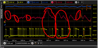
After tested, we found that that register is right, but the waveform isn't correct.


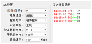
we read the register by the iic tooling.

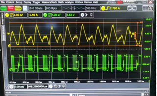
The AVS operation is still held in PFW mode.

So, my question is including,

  1. we rewrote the bit before SOC fully running.  and SBL stage is right?
  2. Is there other operation before and after writing, only the bit2 in 0x04 is ok?

  • Hi Ryan,

    There are currently many questions about your device. Please expect a delayed response from the device expert.

    Regards,
    Megan

  • Hello Ryan,

    From your scope shot, if the yellow represents load current or inductor current, the AVS rail is reacting to a load transient event. During some load transient events, the switch node will turn off temporarily to drain the output cap. This will appear similar to PFM. To confirm the the switch node in FPWM mode, the load needs to be light (less than 300mA) and relatively steady. 

    If you capture the AVS signal as well, you should see the voltage being a little on the high side right before the SW node turns off.

  • Hi Michael,

    Update the testing result:

    Buck2-current:tested by current probe

    Pin 15&16-sw-b2: voltage value of the Pin 15&16(1212), and in front of the inductor 

    This is same as the testing point which was provided last time.

    And what do you mean ' the voltage being a little on the high side right before the SW node turns off' ?

    could you help to explain it in detail?

    Thanks,

  • Hello Ryan,

    After a sudden load drop, the output voltage will increase slightly. When this happens, the Buck's control loop will try to drain some of the charge from the output cap by turning off the switch node. FPWM and Forced Multi-phase mode are easiest to distinguish from PFM/Auto mode at light steady state load scenarios. The left side of your scope shot provides a good example. The BUCK2 current relatively low, and SW is keeping a pretty steady frequency.

  • Hi Michael ,

    As you say, for the sudden load, the voltage will increase. 

    Please refer to the PIC as below, the peak-peak value of AVS more than 60mV while the internal switch turned off.

    Is this a reasonable value(output ripple)?

    For the steady frequency in SW side, it is always changing.

    I marked the frequency in the PIC as below, the value isn't kept  2.2MHz which is setting by register.

    And I captured the SW waveform of 0.85V in 1212, This is steady frequency what I think is right.


    Frequency in 0.85V SW.

  • Hi Michael,

    Update AVS output under low loading.

    After testing, the AVS is still under PFM mode while only Buck1 running. But we have rewrote the register( BUCK1_CTRL Register=0x37) .And the 1212 shall run in PWM operation mode.Is there other operation before and after writing register ?

    Please refer to the PIC as below, is that correct?

  • Hi Ryan,

    We have received your updates and will provide a reply soon. I apologize for the delay once again.

    Regards,
    Megan

  • Is this a reasonable value(output ripple)?

    This is incredibly high output ripple. This is a sign that there isn't enough output capacitance or the FB lines were not routed correctly.

    For the steady frequency in SW side, it is always changing.

    I marked the frequency in the PIC as below, the value isn't kept  2.2MHz which is setting by register.

    The BUCK is experiencing multiple load transient events one after another which doesn't allow the SW to settle. It takes about 20-30us for SW to settle. From your earlier plots that include current, the large load transient events are less than 5us apart.

  • Can you provide a scope shot with 3 channels showing load current, AVS output voltage, and the SW node? It appears to be PWM mode in the left and right side for sure. 

  • Hi Michael,

    Please refer to PICs as below,

    Bcuk1-heavy-Loading: AVS voltage, current, SW Pin

    Bcuk1-Light-Loading: AVS voltage, current, SW Pin

    For the output capacitor and PCB layout issues, could you provide your your email address, I thought I can send our SCH and PCB file to you.

    I hope that you can help to check the our design.

    Thanks,

  • Hello Ryan,

    The device expert is out of office due to holiday in US. Please expect delay in response by tomorrow. 

    Best regards,

    Ishtiaque Panhwar

  • Hello Ryan,

    In the scope capture, the PMIC appears to behave as expected in regards to the SW pin and FPWM mode. Before sending the SCH and PCB files, can you confirm the FB_B1 and FB_B2 are routed differentially to the point of load near the processor?

  • Hi Michael,

    Thanks for your reply.

    We didn't route exactly these two nets as differential pairs. and we have ignored this. Is it root case about this?

    By the way, I have a question as below,

    And I found that new PDN is recommended new design based on TPS6594133A-Q1.  Can 1212+1111 not meet the Soc load ( AVS)? As replying in this item DRA829J: TPS6594-Q1.

    Thanks,

  • Hi Michael,

    Both hevay and slight loading mode are in the FPWM? and could you tell me what the basis to distinguish FPM and loading transient?

  • Hi Michael,

    We also tested Buck1_SW in the EVM-J721EXSOMXEVM, please refer to the PIC as below:

    The phenomenon is the same as ours. how to explain this.

    Thank,

  • We didn't route exactly these two nets as differential pairs. and we have ignored this. Is it root case about this?

    Not routing the FB lines in a good differential pair will have a negative impact on the control loop of the PMIC. This can lead to higher voltage ripple and worse load transient response.

    And I found that new PDN is recommended new design based on TPS6594133A-Q1.  Can 1212+1111 not meet the Soc load ( AVS)?

    The 1212+1111 can still meet the SoC load requirements. However the PDN based on the TPS6594133A has a lower estimated cost and reduced PCB area. Further more, it allows for flexibility in scaling of features such as GPIO Retention, DDR Retention, and MCU Only lower power modes.

  • Large rises and falls in inductor current, signal a load transient event. See circled areas below as example:

    After a load transient event, the buck needs about 16-20us of settle back to normal.

  • We also tested Buck1_SW in the EVM-J721EXSOMXEVM, please refer to the PIC as below:

    The phenomenon is the same as ours. how to explain this.

    Looking at the switch node alone, does not provide enough information. You must look at the Vout for sudden changes indicative of a load transient.

  • Hi Michael,

    Here's buck scope in the EVM. It looks quite similar as ours.

    Do you have a list that describe the differences of solutions in DRA829J: TPS6594-Q1?

    And which Power solution is recommended for TDA4VM-ECO from your side?

    Thanks,

  • Hi Michael.

    Thanks for your replying, and I summarized two items of this problem as follows,

    1. the 1212 cannot stay in PWM mode while SoC transfer into high loading, and then Buck1-3 will be overcurrent warning (I2C reading from 1212). 
    2. And it also seems to be happening in the TI EVM.

    What advice do you have for us fixing this problem?

    Thanks.

  • the 1212 cannot stay in PWM mode while SoC transfer into high loading, and then Buck1-3 will be overcurrent warning (I2C reading from 1212).

    These interrupts can be masked by setting BUCKx_ILIM_MASK=1. Correcting the differential feedback lines and increasing the point of load capacitance will reduce the output ripple and large inductor current spikes.

  • Hi Michael,

    Thanks for your reply.

    So, we should do,

    1. Add more capacitor in AVS power net
    2. Update FB routing
    3. Mask 'current monitoring interrupt' register 

    it cannot be completely fixed, just improved?

    Could you help to share any application note that used to evaluate the Cpol?

    Thanks,

  • If there is adequate capacitance both locally and at the point of load and the FB routing is done correctly, then the ILIM interrupt shouldn't trip. 

    Details on recommendations for buck local and POL capacitors can be found in application section of the TPS6594 data sheet under section 9.2.1.2.5 Buck Output Capacitors. There isn't a separate application note on the subject, but I recommend accounting for all derating factors when picking caps.

  • Hi Michael,

    There is a historical issue here, whey1212 cannot keep PWM operation mode, even if the BUCK1_CTRL Register is update correctly?

    Thanks,

  • Ryan,

    Your scope shots show normal PMIC behavior to load transient events.

    When the load is relatively steady, the buck will switch at a Fsw. When a load transient event cause the Vout to suddenly rise or fall, the buck's control loop will react by temporarily switching faster or slower until Vout is back on target. This is normal behavior. 

    -Mike 

  • Hi Michael,

    Thanks for you explaining more detail how to solve this problem.

    -Ryan