This thread has been locked.

If you have a related question, please click the "Ask a related question" button in the top right corner. The newly created question will be automatically linked to this question.

TPS54226: switching frequency jitter

Part Number: TPS54226

Hi Experts

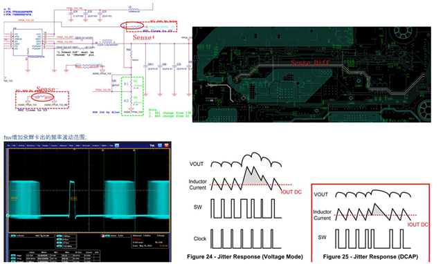
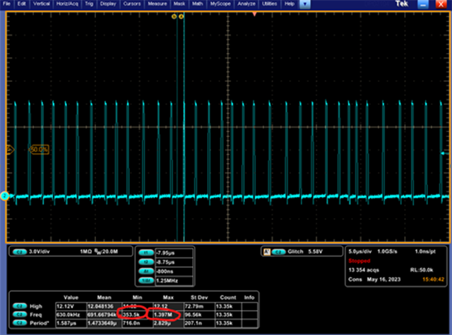
our customer find switching frequency have jitter. datasheet is 700kHz  but when they use long time .

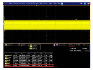
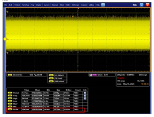
frequency maximum value would be 1.397Mhz and minimum is 353.3kHz.

customer have four question want to check with you

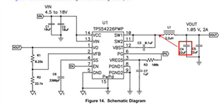
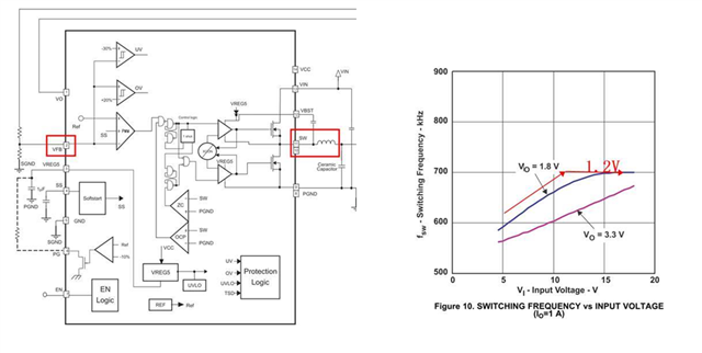
1. switching frequency range.

2. which reason will influence jitter.

3. if the range of jitter is too large . would it influence IC life cycle?

4.if VFB pin is disturbed , would it influence SW pin?

best

regards

brian

  • Hi Experts

    attached file is layout and SCH

    TPS54226_1.2V_SCH_20211026a.pdf

    https://e2e.ti.com/cfs-file/__key/communityserver-discussions-components-files/196/TPS54226_5F00_1.2V_5F00_Debug_5F00_B_2D00_0225.brd.7z

    Our customer add one pairs remote sense line. do you know the proper range of frequency ups and downs?

  • Hi Brian,

    Yes these devices tend to have higher jitter than the voltage mode or current mode counterparts. I checked your schematic and layout and have the following suggestions. Btw, what is the output current at which the SW measurement is done? Do you have the VO ripple measurement also?

    • Please separate out the VCC and VIN connections in layout.
    • Please bring in the output caps on the other side of the inductor closer to the IC.
    • And likely cause of the jitter you observe is the VO trace which is very near the inductor SW node. Please route it further away - check EVM example figure 3-5 (https://www.ti.com/lit/ug/slvu336a/slvu336a.pdf#page=11) and also if possible, the trace can be on bottom layer.
    • You can try out the same design on an EVM to see if the measurement setup is an issue or not in terms of noise introduced.

    Thanks,
    Amod

  • Hi Amod

    • Please separate out the VCC and VIN connections in layout.

    our customer have layout already. and they previous layout also connect Vout and VCC. They do not meet this problem.

    • Please bring in the output caps on the other side of the inductor closer to the IC.

    do you mean move Capacitance to SW pin?

    • And likely cause of the jitter you observe is the VO trace which is very near the inductor SW node. Please route it further away - check EVM example figure 3-5 (https://www.ti.com/lit/ug/slvu336a/slvu336a.pdf#page=11) and also if possible, the trace can be on bottom layer.
    • You can try out the same design on an EVM to see if the measurement setup is an issue or not in terms of noise introduced.

    (P01 remove Sense VO to GND ripple 5.3mV,test VO pin)

    (P02 Connect Sense VO to GND ripple 154mV,test VO pin)

    (P03 Connect Sense VO to GND ripple 23.2mV,test load)

    sense line impact VO and fsw jitter more.


    could you give me a detailed range of Dcap fsw jitter that IC can afford it ?  

    Thx for your support Slight smile

    Best

    Regards

    Brian

  • Hi Brian,

    Suggestions 1 and 2 on VCC/VIN and output cap placement are guidelines in general. If the layout is working from before, you may proceed as is. On the DCAP FSW jitter, in general, a 20% or even higher variation in switching period (rising edge of SW to next rising edge of SW) is quite normal. We do not have exact range but you can use this number to estimate a range. 

    On the waveforms you share, are those on the EVM or the custom board? It will be a good idea to have the VO sense line further away from SW as mentioned before.

    Thanks,

    Amod