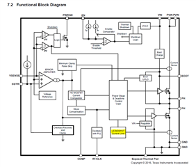
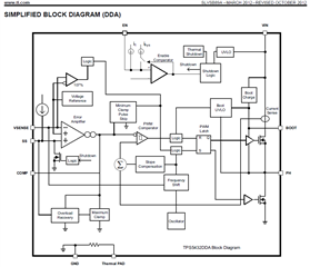
Other Parts Discussed in Thread: TPS54620
Hello,
I'm currently trying to debug a problem with a relatively old design of my company.
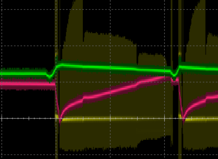
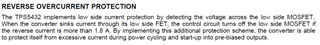
this old design is re-used in a new project, but now we are getting a repeated returns from the field with failure of the buck converter chip TPS5432. All the boards show the same failure mode, the PH Pin (Pin 3) is short circuited to GND (Pin 4)
here is a snapshot of the circuit
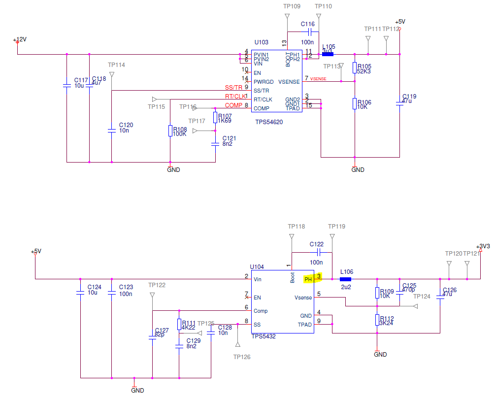
The Chip is very lightly loaded, it is used to power an AVR micro-controller and a temperature sensor.
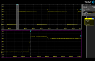
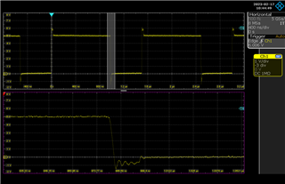
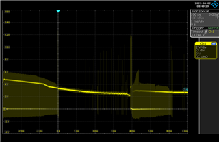
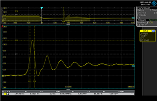
I've been trying to reproduce the failure in lab for weeks now but with no success so far.
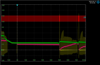
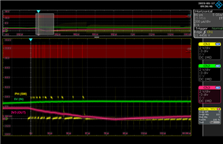
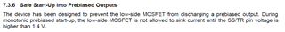
I've came across your application note SLUA962, but I couldn't reproduce the problem with the scenarios mentioned in it.
I'm wondering if you could help me with other possible root causes of this failure mode, or if you have a known issue or similar reports about this chip.
Best Regards
Moamen