This thread has been locked.

If you have a related question, please click the "Ask a related question" button in the top right corner. The newly created question will be automatically linked to this question.

BQ76942: LD pin with large resistor

Part Number: BQ76942
Other Parts Discussed in Thread: TIDA-010208

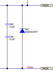
The customer used 6000uf in the PACK+ and PACK-.

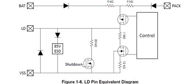
When the customer want to enter shutdown mode, it will last too much time until the LD pin voltage decreased to VWAKEONLD.

So in the LD pin, the customer want to use larger resistor like 1M instead of 10k, and then the detected voltage level will be below VWAKEONLD.

Besides, Set "protections load detect:active time" to 0 for the normal operation of OCD latch and SCD latch.

If the customer choose this design, is there any other risk not in the consideration?

Thanks

  • Hello Fabio,

    We typically recommend 10k-Ω for PACK and LD pins. These pins have internal resistance of 600k-Ω and 2M-Ω respectively.

    This thread shares good info. LINK

    Regards,
    Jose Couso

  • So I guess larger resistance is needed like 10M even 20M.

    The issue is the PACK+ voltage decrease too slow until VWAKEONLD (Nearly 2 hours) when they system need to enter shutdown mode.

    So the customer want to use higher resister in the LD pin so that the LD pin voltage is always lower than VWAKEONLD.

    And then disable the load detection function.

    Could this solution work?

  • Hello Fabio,

    Larger resistances will create a voltage divider and LD pin will not sense the correct voltage. 

    The issue is the PACK+ voltage decrease too slow until VWAKEONLD (Nearly 2 hours) when they system need to enter shutdown mode.

    This sounds like a capacitive behavior to me. You mentioned they have 6000uf in the PACK+/-. Can they try reducing this to a few micro Farads? TIDA-010208 reference design uses two 0.1uF in series.


    Please share their schematics.

    Regards,
    Jose Couso

  • Because the customer only is responsible for the pack, the 6000uF is in the system side. And the system side would not like to change their design.

    The battery is unremovable, so the customer do not need the load detection function. So they will close the load detection function.

    1. Considering the usage situation, can you help to recommend an appropriate resistance value?  Just let the LD pin voltage always lower than VWAKEONLD.

    2. I noticed the pin equivalent diagram, which seem do not match the internal resistance you mentioned. Could you explain this?

    We typically recommend 10k-Ω for PACK and LD pins. These pins have internal resistance of 600k-Ω and 2M-Ω respectively.

  • Hello Fabio,

    1- Having a large resistor at the LD pin would not make a huge difference since LD is referenced to the IC GND (in our Evaluation module). 

    One solution would be to ground the LD pin to PACK-, so when the DSG FET turns OFF, the device shutdowns immediately. If they use this solution, they would need to use a forward biased Zener diode from PACK+ to the gate of the DSG FET to not damage the FET when  PACK goes to zero (this is shown in our Evaluation module). 

    Note: An explanation of how DSG FET turns OFF can be found in Section 8 DSG Driver of the Multiple FETs with the BQ76952, BQ76942 Battery Monitors.


    2- I forgot to include "effective" internal resistance. So, no all the resistances seen from the pins are shown in the block diagram.

    Note: The LD pin has an internal resistance of 80kΩ when in shutdown mode.

    Regards,
    Jose Couso

  • Hi Jose, the customer has decided to ground the LD pin to PACK-. 

    They want to know whether 10kΩ is needed? Or  just grounded directly? Or other resistance?

    Could you please give some comments?

  • Hello Fabio,

    The 10kΩ is not needed. They can just ground the LD pin directly to PACK-.

    Regards,
    Jose Couso

  • We ground the LD pin directly to pack-, when charge mosfet is off (Over voltage protection),we apply a 45V voltage at pack+, and we find the CHG pin voltage will higher than BAT pin voltage , and it will continue to increase if we increase the pack voltage ,finally, charge moseft will be turn on or demaged. if we connect LD pin to pack+ with a 10k resistor, there is no this issue.why the LD pin caused this issue?

  • Hello Duncan, 

    I am assigning this thread to the expert of the device.

    Regards,
    Jose Couso

  • Hello Duncan,

    Is the DSG FET on or off?

    If the LD pin is grounded, voltage applied through the PACK+ that could leak to the DSG pin can potentially pull-up the charge-pump voltage higher to the DSG voltage. This is likely what you are experiencing, in order to avoid this problem we would recommend to not ground the LD pin, or to ensure that no high voltage is being seen at the DSG pin. 

    Best Regards,

    Luis Hernandez Salomon