This thread has been locked.

If you have a related question, please click the "Ask a related question" button in the top right corner. The newly created question will be automatically linked to this question.

TPS2061: Questions about reverse power

Part Number: TPS2061
Other Parts Discussed in Thread: , TPS2065C

Hi - I'm using the (correction:) TPS2061CDBVT to control power to the USB OTG connector.
I can read/write to a USB stick (board in host mode), and read/write to a PC USB-CDC (board in device mode).
The board normally has its own power and is not powered from the PC.
However, a couple questions:

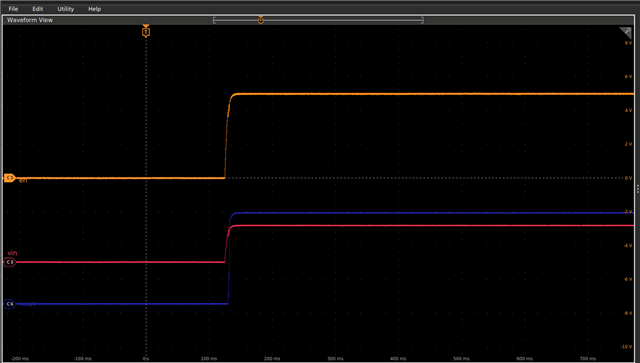
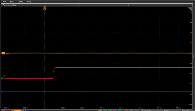
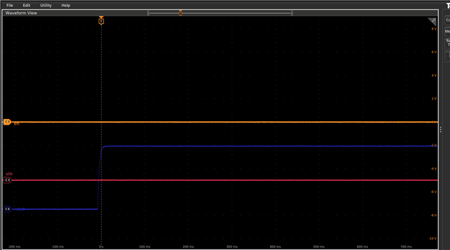
1) What happens if the board power is disconnected while it is connected to the PC?
Power flows happily from PC to board 5v, as the switch is bidirectional? Or???

2) What happens if the user plugs into the PC without first applying board power?

Thanks in advance!
Best Regards, Dave

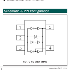
PS: If Bad Things happen, what protection or alternate circuit should I use?

USB_power_circuit.PNG

  • Hi Dave,

    Assign to Eric, who is responsible for US.

    Best Regards,

    Kuno

  • Hi Dave,

    The switch is designed to control power from IN to OUT.  That is, it's not meant to be bidirectional.  I have doubts TPS2061 will block reverse current since the datasheet doesn't make any claims to do so.  In a scenario where the board is unpowered but 5V is present on USB VBUS, the worst thing that could happen is current flows through the integrated FET's body diode, resulting in ~4.3 V on IN.

    It sounds like you are looking for is reverse current blocking.  There's a good app note on the subject here: https://www.ti.com/lit/an/slva730/slva730.pdf.  The most comparable device to TPS2061 with guaranteed reverse current protection is TPS2061C.  It will block reverse current whenever the switch is disabled, meaning IN pin will stay at 0V.

    Regards,
    Eric

  • I.m confused. I am using the TPS2061DBV, TPS2061C is different??

    I'll have a look at the app note in the AM, Thanks!

  • Hi Dave,

    I guess Eric is right, we can have a test for you to confirm that, but we don't have the EVM now, I will submit a request for it, and I will have a test for you next week, thank you.

    Best Regards,

    Kuno

  • UPDATE: the part we are currently using IS TPS2061CDBVT.
    A few months back I got an older datasheet from DigiKey web site - they have fixed this.
    So, I am ALREADY using the part you suggested.
    Apologies for the confusion...

    Now I'm confused. Why did PC power the board when board power was removed?

    Thanks!

    Thanks Eric - I read the app note and looked at the TPS2061C data sheet.
    Can you confirm TPS2061C does reverse current blocking even when un-powered?
    I'm afraid that is not clear in the datasheet.

    If TPS2061C does in fact block reverse current when not powered,
    I can just use this part to replace the original (non "C") with no changes?
    We do not need to power the board from PC.

    Thanks again for the help,
    Best Regards, Dave

  • Dave,

    TPS2061/TPS2061C are functionally drop-in replacements as long as you're selecting the same package variant.

    You are saying if you apply 5V at OUT, it gets passed through to IN?  This is not what I would expect.  I expect the signal should get blocked at OUT, even if the device is unpowered.  Kuno can confirm when he receives his test hardware.

    Regards,

    Eric

  • Again, we are already using the TPS2061CDBVT.
    Never did use the earlier part.
    Apologies again for the part number confusion...

    Yes, when board power was disconnected, PC powered board until USB cable was unplugged.

    I am really confused as to what is happening here.
    Thanks for any light you can shed on the issue,
    Best Regards, Dave

  • Hi Dave,

    I use the TPS2061EVM and TPS2065CEVM(only EN high different  with TPS2061C), and when I input the voltage to the output, and measure the input pin voltage, it is 0, so it should not happen what you meet, so I guess it may have some other way that let the current go from output to input, could you please remove our device and check the input again?

    TPS2061:

    1, EN=low, and power on the input=5V, then output=5V

    2, EN=high, and power on the input=5V, then output=0V

    3, EN=low, and power on the output=5V, then input=0V.


    TPS2065C:

    1, EN=high, and power on input=5V, then output=5V,

    2, EN=low, power on input=5V, then output=0V

    3, EN=low, power on output=5V, then input=0V.

    Best Regards,

    Kuno

  • Thanks for checking. I'm still confused what's going on with my design. I did find an error, but I don't think it is contributing to the problem and I don't think it damaged the switch. If you look at my schematic, I used a TVS diode array with the supply side of the TVS tied to the switch output. This is wrong because the OTG_ID pull-up pulls the switch output up to .7v (1.4v at OTG_ID, one diode drop in TVS array, 2nd diode drop in switch output). TVS array V_supply should be connected to (unswitched) 5v supply so this does not happen.

    Can you confirm this is unlikely to have bothered the switch?
    With 10k pull-up to 3.3v, back current through switch is only (3.3v-1.7v)/10k = .2ma

    Thanks!
    Best Regards, Dave

  • Hi Dave,

    I am not very clear about you description, you mean the 'TVS array' is the RCLAMP0503F.TCT, but I also check its datasheet, I can not find the current path, could you please help me describe it in the below picture? From which pin to which pin? Thank you.

    Best Regards,

    Kuno

  • Sure  - Current flows through R10 pull-up, into SIGNAL_3 pin 3 and out pin 5 (1 diode drop), through FB13, into switch output (2nd diode drop). Hence OTG_ID sits at 1.4v and does not pull high. This also means switch !EN is sitting at 1.4v, but switch is still off (data sheet says switch won't turn on until !EN down to .7v). Hope I explained OK, Thanks!

  • Hi Dave,

    Kuno is currently out of office, but I am able to take a look at this.

    I am also not sure I understand your concern with OTG_ID.  If PC connects while system side is unpowered, I expect V5V0 and V3V3 to be 0V.  VBUS = 5 V (from PC) and ID = 1.4 V.  Both diodes regarding clamp pin 3 are reverse biased.

    Since ID and !EN are the same net, !EN = 1.4 V.  This is right at the logic threshold of the pin, but it shouldn't matter since IN < UVLO.  From section 8.3.3: "The MOSFET power switch blocks current from OUT to IN when turned off by the UVLO or disabled."

    Based on all this, I expect the following voltages at TPS2061C when a PC is connected without system side power:

    • OUT: 5V (VBUS from PC)
    • GND: 0V
    • !EN: 1.4 V (OTG_ID from PC).  This also assumes it can drive the 10k resistor on V3V3
    • !FLT: Hi-Z (Section 8.3.5: "FLT is high impedance when the TPS20xxC and TPS20xxC2 are disabled or in undervoltage lockout (UVLO).")
    • IN: 0V

    Please let me know if I'm misinterpreting the scenario.

    Regards,
    Eric