This thread has been locked.

If you have a related question, please click the "Ask a related question" button in the top right corner. The newly created question will be automatically linked to this question.

TL494: Min ~ Max range for maximum duty cycle

Guru 19645 points
Part Number: TL494
Other Parts Discussed in Thread: TL431

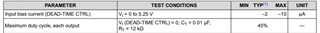
Datasheet P6 is described maximum duty cycle at typ.

Is there min and max value for maximum duty cycle.

Also, please let me know variation in the case of 90% duty cycle (DTC: GND, OUTPUT CTRL: GND).

【Background】

I investigating the reason for become 85% duty cycle, not so target of 90% on boost application. 

I have listing up other possible causes(Inductor, accuracy of external, etc), but I would like to confirm the Min~Max range in the maximum Duty cycle, too.

Best regards,

Satoshi

  • Satoshi,

    The min/max range of duty cycle is not a measured parameter and this is why you only see a typical max of 45% and even this number is specified for VCC=15 V and f=10 kHz. You should try and set up the oscillator RT and CT as close to the yellow highlighted line (0 %) shown below and also, make CT small as possible and RT large.:

    Regards,

    Steve M

  • Hi Steve

    Thank you for reply,

    Customer's request spec is VCC:15V, CT: 0.001μF, and RT: 10kΩ, equal to 100kHz.

    Is 100kHz can not make nearly 0% variation, is it correct?

    Would you let me know if there any idea for high accuracy 100kHz?

    By the way, is CT not recommend for less than 0.001μF?

    Best regards,

    Satoshi

  • Satoshi,

    The programmed frequency of 100 kHz using the RT, CT values you provided, is nearly off the log graph. I would say 85% is good using TL494. If you have already tried the smallest possible CT and you have made the DT as small as possible, the only recommendation I make to improve the accuracy is to try a different double-ended PWM controller. Depending what features are most important, you can search from the parametric list shown here.

    Regards,

    Steve M

  • Hi Steve

    Thank you for advice,

    I understood.

    I'm investigating how to calculate the worst case duty ratio.

    Would you let me know the minimum value of input threshold voltage for Zero duty cycle, for the information I want to know for the investigation?

    The data sheet only described Typ: 3.0 and Max: 3.3V.

    Best regards,

    Satoshi

  • Satoshi,

    The reason the minimum input threshold is not specified is because it is not a measured parameter according to ATE test.

    Regards,

    Steve

  • Hi Steve

    Thank you for reply,

    Sorry for additional question,

    I am researching and calculating duty_max limit.

    However, even if I assume the large worst case margin, it was not reach the Duty: 85% (real waveform).

    I believe the following affects the limits of Duty.

    Would you let me know If there are any other points (specs) or mistakes that affect Duty?

    ⇒Dead time offset: 0.1V (-3%), relation for Rt and frequency (100kHz → over -2%), Internal Transistor's tr: 200ns, tf: 100ns, comparator delay: 400ns

    Best regards,

    Satoshi

  • Additional delays coming from the power stage should also be considered. For example, MOSFET turn-on delay, gate drive rise/fall delay, xfmr and MOSFET dv/dt, etc.

    Steve

  • Hi Steve

    Thank you for reply,

    The output pulse of E2 (10 pin) is already Duty: 85%.

    Are there any other points that affect Duty in TL494?

    Best regards,

    Satoshi

  • Satoshi,

    TL494 is voltage mode control. From the PWM point of view, only the CT voltage (RAMP) and FEEDBACK are used to determine duty cycle. Make sure you have a clean CT signal at the oscillator, make sure the FEEDBACK is clean (no switching noise or spikes). The only thing determining the duty aside from the PWM is the power stage and we already addressed where the possible delays within the power stage could be coming from.

    Regards,

    Steve M

  • Hi Steve,

    Thank you for advice,

    I update the confirmed contents below.

    ・Confirmed the CT voltage and Feedback.

          A slight noise occasionally appeared, but the Duty: 85% regardless of the noise.

    ・I tried to pass the driver circuit and operate the FET directly, but the duty was still 85%.

    In conclusion, is it impossible to configure 36Vin to 380Vout with TL494?

    Best regards,

    Satoshi

  • Satoshi,

    36V<VIN<380V is 10.55:1 ratio. This means you have D=85% for VIN=36V, you should have D=8% for VIN=380V. For VMC, your DC voltage gain will vary over such a wide input voltage and this means your regulation accuracy may be less when operating near min/max VIN. Also, check the condition for VIN=36V, D=85% and check the feedback. If an optocoupler used - is the optocoupler TL431 biased correctly? Optocoupler/TL431 is an important part of the feedback circuit and you need to make sure there is sufficient dynamic range for the range of input voltage, output load you need to cover? 

    Steve