This thread has been locked.

If you have a related question, please click the "Ask a related question" button in the top right corner. The newly created question will be automatically linked to this question.

BQ76952: Power management forum

Part Number: BQ76952
Other Parts Discussed in Thread: UCC27524

We HAVE BEEN TRYING TO DESIGN A 14-16S bms. We have been referring to the design document named TIDA 010216. In this document, we came across a charger detect and a charger reverse circuit. (I have attached the images). Could you please give small notes and directions with respect to the functionality of these two circuits so that we may know their purpose in the whole scheme of things   

  • Hi, 

    I have looped our engineer here to help you, please expect feedback by this week.

    Ryan Tan

  • Hi

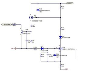
     About the circuit of picture that you attached,  which is mainly used for charger detection and load detection. the second picture you attached that is used to detect if a charger is connected.  for example, if your system is 48V and due to system load discharge, the Bat voltage is now 30V, if a 48V charger is connected at this time. the GND will be higher than PACK- voltage,  this action will turn on Q36, and then, due to voltage divider resister will cause  Q31 to open. at the same time, Q30 is also turn on, the CHG WAKE will pulldown to GND,  the CHG WAKE is connect to the MCU, when the MCU receive the signal of the CHG WAKE pulldown to GND, MCU will enable FET driver UCC27524 to turn on MOS FET to charge.

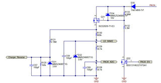
    the first picture you attached, which is used to load detection and charger reverse detection,  PACK_EN is connect to the MCU, if you system want to detect, the MCU will enable PACK_EN,   if your charger is reverse, the PACK- will have a large voltage.  Through charger reverse connect to the MCU ADC, the voltage of ADC show if a reverse charger is connected.   in addition, if your system is connected to load,  the LD WAKE will be detected votage is close to GND, so to determine if there is load access.

  • Hi Yebhor

    the designation of the transistors i.e q36,q35  etc., are not clear. I think it might be mentioned with some other designation. Also ,Please give us a more clarity. We could not understand the explanation which you have given

  • Hi 

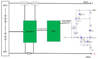
    for charger detection circuit ,  i drew a sketch, such as the left picture. Assuming you have a 48V system, now due to system discharge,  the battery voltage is 30V,  so you need to connect a  48V charger.   when the charger connect to the PACK+ and PACK-,  Due to the parallel connection between the charger and battery pack, GND will be 18V higher than PACK-, therefore, if a charger is connected, the Q36 N-MOS will be open,and then Q35 P-MOS will be open,  and then Q34 transistor will open, and the CHG WAKE will be pulled to GND, at this time, MCU receives a pull down signal and wake up AFE to open the high side MOS for charging.

    if you have a load is connected to the PACK+ and PACK-, and PACK_EN is enabled by MCU.   the LD_WAKE connect  to the MCU ADC which will collect specific voltage,  and then MCU will wake up AFE for discharging. in addition,  if your charger is reversed, a large voltage will appear when connecting the Charge_ Reserve to MCU ADC to determine the charger`s reverse connection. if it is reversed, the MCU will give an alarm.

    Best Regards

    Yebohr zhao 

  • Thank you so much Yebohr