This thread has been locked.

If you have a related question, please click the "Ask a related question" button in the top right corner. The newly created question will be automatically linked to this question.

TPS54A20: About the specifications of each pin

Part Number: TPS54A20

Hi, TI expert.

There are 7 points that I would like to ask you to teach, such as the tolerance of the SS/FSEL comparator and the use of SCAP.

1. When running with RSS/FSEL 21.5kΩ, what is the SS/FSEL value? Should it be within 21.715-21.285kΩ which is ±1% from 21.5kΩ, or is 22kΩ acceptable?

2. How many MHz can the SYNC pin drive? Min_Ontime is 20ns, if the input voltage is 8V and the output voltage is 2V, is it possible to operate at a switching frequency of 12.5MHz and an actual operation of 25MHz?

3. Also, is it okay to open SYNC when moving with SS/FSEL?

4. VGA also has a regulator like VG+, but if a separate voltage is supplied here as well, will the efficiency be improved?

5. I apologize for asking an amateur question, but I understand that BOOTA and BOOTB have capacitors for switching operation, but what is the purpose of SCAP?

6. Why is the capacity of the capacitor connected to BOOTA, B 0.047uF?

7. Why is the capacitor attached to SCAP 2.2uF? If you only refer to the rise time, shouldn't you choose a capacitor with a smaller capacitance?

best regard.

  • 1. When running with RSS/FSEL 21.5kΩ, what is the SS/FSEL value? Should it be within 21.715-21.285kΩ which is ±1% from 21.5kΩ, or is 22kΩ acceptable?

    Resistors should be 1% tolerance resistors with the listed nominal value.  This ensures the desired selection option over the operational tolerances of the device.   Selecting a different nominal resistor value may result in some devices selecting a different option than intended.

    2. How many MHz can the SYNC pin drive? Min_Ontime is 20ns, if the input voltage is 8V and the output voltage is 2V, is it possible to operate at a switching frequency of 12.5MHz and an actual operation of 25MHz?

    SYNC function is rated for a maximum of +10% over the programmed frequency.  The programmed frequency has a maximum of 5MHz per phase for a total of 10MHz switching frequency.  The maximum SYNC frequency is 11MHz.

    3. Also, is it okay to open SYNC when moving with SS/FSEL?

    Yes

    4. VGA also has a regulator like VG+, but if a separate voltage is supplied here as well, will the efficiency be improved?

    The VGA regulator is not reference to GND, the VGA regulator is referenced to SCAP.  It is not recommended that users contract an external supply referenced to SCAP to externally power VGA.

    5. I apologize for asking an amateur question, but I understand that BOOTA and BOOTB have capacitors for switching operation, but what is the purpose of SCAP?

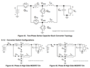
    SCAP is a series switched capacitor that is reducing the voltage stress on each MOSFET and switching node. the SCAP capacitor maintains a VIN/2 voltage so that each switching node sees no more than 1/2 of the input voltage.  The lower switching voltage reduces switching losses and improves efficiency at the high switching frequencies that the TPS54A20 switches at.

    6. Why is the capacity of the capacitor connected to BOOTA, B 0.047uF?

    These boot-strap capacitors power the internal drivers and MOSFET gates for the high-side MOSFETs on SWA and SWB.  They are sized to provide acceptable levels of BOOT discharge during the turn-on of these MOSFETs.  0.047μF is selected based on the gate charge of the MOSFETs and internal loading of the driver circuitry powered by BOOT.

    7. Why is the capacitor attached to SCAP 2.2uF? If you only refer to the rise time, shouldn't you choose a capacitor with a smaller capacitance?

    SCAP provides the charge for each of the two channels during their high-side on-time.  2.2μF is selected to provide good performance across the operating range of the TPS54A20.  A smaller SCAP would allow more ripple voltage on SCAP during each switching cycle.  Increased ripple voltage on SCAP results in higher voltage stresses and increased switching losses, reducing efficiency.

  • I apologize for the delay in replying due to the time difference.

    Thank you very much for your very clear explanation.

    I have only one question.

    >the SCAP capacitor maintains a VIN/2 voltage so that each switching node sees no more than 1/2 of the input voltage.

    That means when Vin12V, Vout2V, fsw5MHz,

    Ontime is 66.7ns, or 33.3ns?

    1/5MHz = 200ns

    2V/(12V/2) →200ns/3=

    Will it be 66.7ns?

    Or

    2V/12V →200ns/6=

    Will it be 33.3ns?

  • Hi,

    Peter will check your question and reply you soon.

  • >the SCAP capacitor maintains a VIN/2 voltage so that each switching node sees no more than 1/2 of the input voltage.

    That means when Vin12V, Vout2V, fsw5MHz,

    At 5MHz per phase, 12V input to 2V output, the on-time will be 200ns * (2V / (12V/2) ) = 200ns * 1/3 = 66ns

  • Thank you Miranda.

    Gomi,

    Here is the switching block diagram for the 2-phase switched capacitor  BUCK converter from page 22 of the datasheet https://www.ti.com/lit/ds/symlink/tps54a20.pdf#page=22 

    When switch Q1a is on, SCAP is pulled up to VIN and SWa is pulled to VIN - Vscap, which is VIN/2

    When switch Q1b is on, Q2a is also on, and SWb is pulled to SCAP, which is also VIN/2

    With the "ON" time voltage on each switching node VIN/2, the duty cycle is 2 x Vout/Vin  and the on-time is 2x Vout/Vin x 1/Fsw 

  • Thank you peter.

    Sorry for asking so many questions, but I have one question.

    1. Are the potentials of SWA and SWB approximately Vout + Iout × ωL?

  •  

    The average voltage of the switching nodes SWA / SWB are approximately Vout + Iout/2 x (DCR + Rtrace)

    Where DCR is the DC resistance of the inductor and Rtrace is the trace resistance from the switching node to the regulated output voltage.

    Each switch node and inductor is carrying 1/2 of the total output current, so the voltage drop across the inductor is based on 1/2 of the load current.  Also, the average voltage doesn't change much with frequency, so it doesn't really follow ωL, but stays with DCR.

    The dynamic voltage of the switching nodes SWA / SWB is that:

    SWA is approximately VIN - (Iout/2 * RdsonQ1a + Vscap) during the Q1a "On-time" and approximately - (Iout/2 * RdsonQ2a) during the Q2a "On-time"

    SWB is approximately Vscap - Iout/2 * RdsonQ1b during the Q1b "On-time" and approximately - (Iout/2 * RdsonQ2b) during the Q2b "On-time" 

  • thanks so much.

     I understand very well.

    Thank you for your continued support.