A related question is a question created from another question. When the related question is created, it will be automatically linked to the original question.
If you have a related question, please click the "Ask a related question" button in the top right corner. The newly created question will be automatically linked to this question.
Can you share the TPS546D24A Compensation and Pin Strap Calculator excel file that you used to generate the design along with the schematic snips that you shared?
Dani Nadira is reviewing your schematic and excel worksheet. If you are able to provide a more complete schematic, she can provide a more complete schematic review, but is reviewing what you have provided.
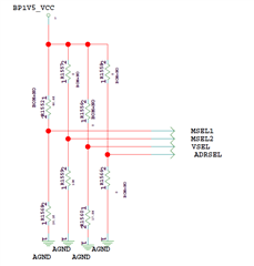
The resistor programming of VSEL shown in your schematic does work for VOUT = 0.85V. However, there was a discrepancy in the way VOUT range was entered in your excel worksheet. You should enter it as 0.5 to 1.25V at 0.05V resolution to correspond with the resistor code you chose; it was entered as 0.75 to 0.89V at 0.01V resolution, which would also work for VOUT = 0.85V but does not match the VSEL resistor programming in the schematic.
Your Iout = 22A is less than 30A, and Vout ripple = 10mV is less than your desired 3% max ripple, which looks good. However, your MSEL1 programming is not resulting in your desired switching frequency and compensation code. Since there is no resistor to BP1V5, the switching frequency is 550kHz, not 900kHz. The R2G code also results in compensation code 18, which has a current loop gain of 5 that would be too high and result in instability. For a switching frequency of 900kHz and compensation code 4, you should program MSEL1 with Rbot = 10kΩ and Rtop = 4.42kΩ.
I have reviewed your schematic and everything looks good. Here are a few comments:
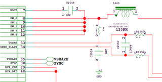
-I was unsure of your values for VCC_IO and EN because their specific voltages were not included. For VCC_IO, make sure that the voltage is between 1.8V and 5.5V. Voltages less than 1.8V may be hard for the PMBus to differentiate as high vs low, and anything larger than 5.5V exceeds the max allowed voltage for PMBus and risks damaging the part. For EN, make sure the voltage is between 1.1V and 5.5V. Also, the VCC12 label makes it seem that Vin=12V, I just wanted to bring it to your attention since I know you mentioned you were using Vin=6V.
-If SYNC is being sent out to another circuit, you may want to consider updating the resistors of ADRSEL to the SYNC OUT configuration rather than Auto Detect
-I would recommend adding a 0-Ω placeholder resistor on the BOOT pin in series with C2548. Having a resistor here in series would slow down the turn-on of the high-side FET which reduces the energy that causes ringing on the switching node. It has a similar benefit as the snubber with less power dissipation. You can evaluate the ringing on the SW pin after layout to see if it would be necessary. I would recommend a max of 4.7Ω for the resistor if used
-As a general comment for layout, make sure when connecting AGND to PGND, use a thick trace underneath the part from the AGND pin to the exposed pad
That sounds great. If this has resolved your issue, please click "This has resolved my issue" to close the thread. If you have any additional questions, please create a new thread and we would be happy to help.