


Hi,
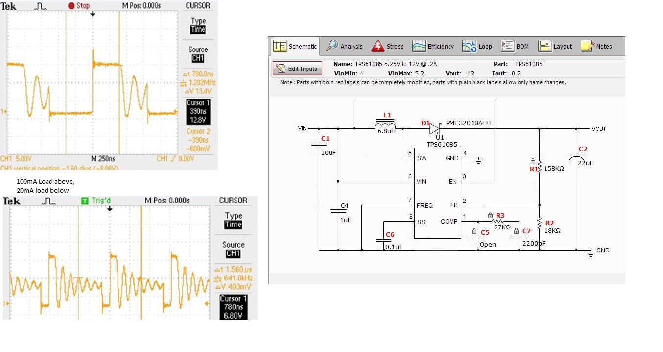
I have a concern about the signal I am observing at the SW pin on the TPS61085.
my circuit has been designed to supply a maximum 200mA and I find when the load is nearing this value the signal at the switch pin is very clean (no oscillations or bumps as they are referred to in application note SLVA381 "Simplifying Stability Checks by John Stevens")
I designed the circuit using Switcher PRO software, it calculates a Gain Margin of -18dB , phase margin of 74 degrees, when I use a 10uF ceramic Capacitor on the output
However even with these low ESR capacitors I noticed when the load begins to slowly decrease over a minute or so, the oscillations starting to increase in quantity at the SW pin to a maximum when my load has reduced to 20mA (as shown)
It is not difficult to reduce the oscillations at a particular load by changing the capacitance on the output. however in practice my load is going to vary.
Is it possible to remove these oscillations for a load that varies over a range (20mA to 200mA in my case)?
Based on the attached images, are these oscillations acceptable or are there risks associated with leaving the design as is?


