Hello,
My customer inquires for additional information required for system design.
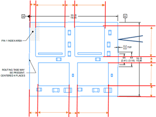
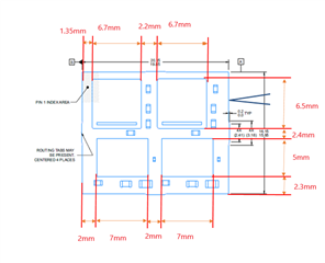
Could you please give them the height information shown in red below?
Thank you.
JH
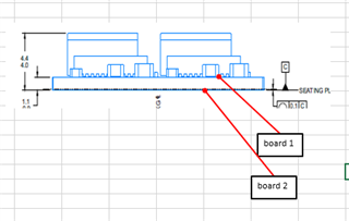
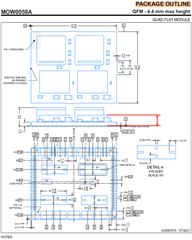
Hello,
My customer inquires for additional information required for system design.
Could you please give them the height information shown in red below?
Thank you.
JH