This thread has been locked.

If you have a related question, please click the "Ask a related question" button in the top right corner. The newly created question will be automatically linked to this question.

LM5146: Routing HO and LO under Bootstrap cap and VCC-GND cap

Part Number: LM5146

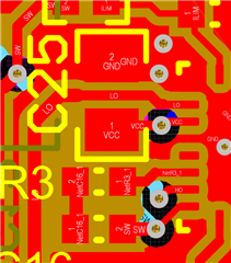
I am currently designing a PCB with an LM5146 and am using the LM5146Q1 development board as a reference. The schematic of the PCB shows TI routing the LO output of the IC under the VCC-GND cap. However, the HO output of the IC is routed with a via because TI uses a resistor in series with the bootstrap capacitor. If I only use a bootstrap capacitor with pads of sufficient separation, am I able to route the HO output under that capacitor without issue? Why or why not? Here is a picture for reference.

  • Hi Paul,

    Thats fine yes. However HO should route differentially with SW as it does internally on our board.

    Also, HO and SW are high dV/dt nodes, if you have long traces on the top layer then they can act as antennae and radiate EMI.

    Thats the reason we usually route those internally and then only via at the FET and IC.

    Hope this helps,

    -Orlando