This thread has been locked.

If you have a related question, please click the "Ask a related question" button in the top right corner. The newly created question will be automatically linked to this question.

TPS40428: PWM abnormal and may cause large current

Part Number: TPS40428

Hi TI Team,

I have some re-spin PCBs return but I found the chip performance is not very stable now.

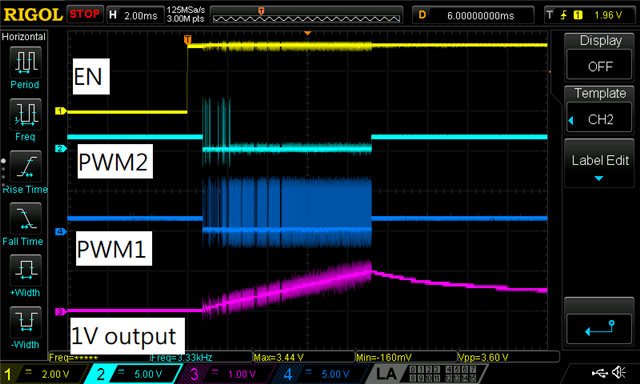
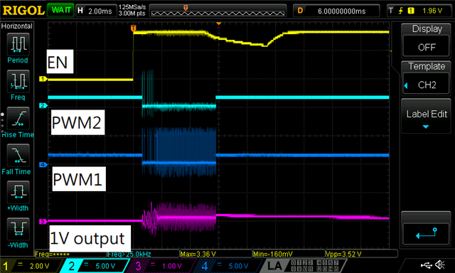
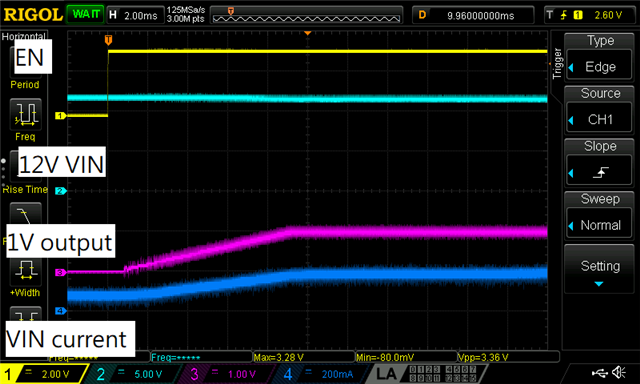
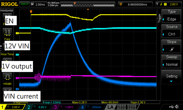
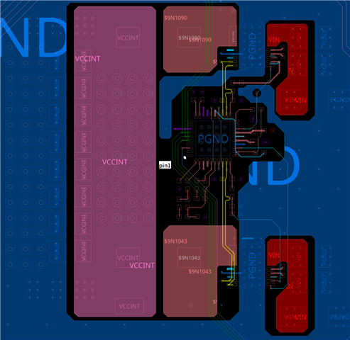
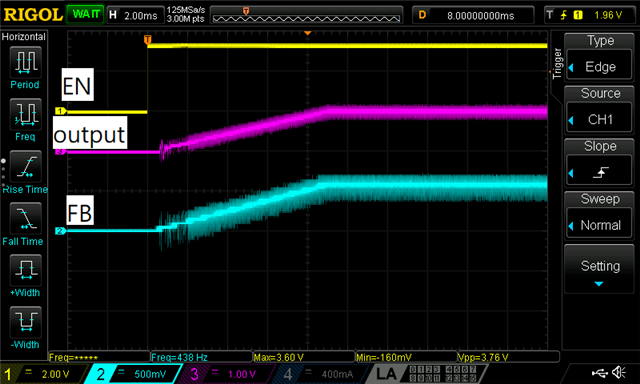
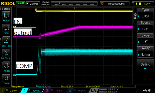
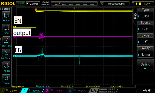
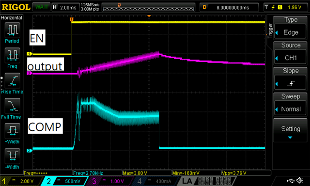
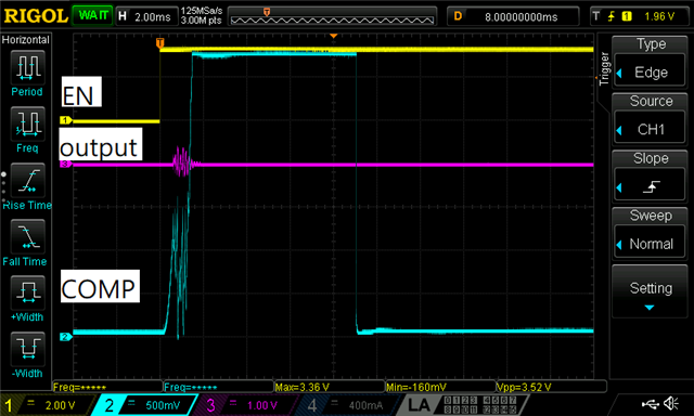
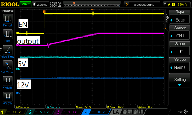
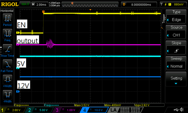
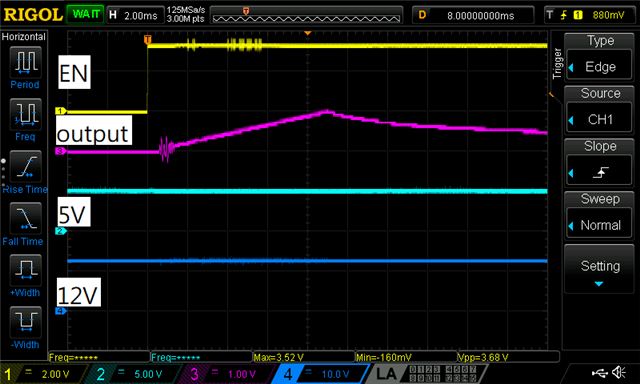
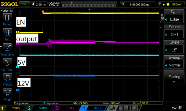
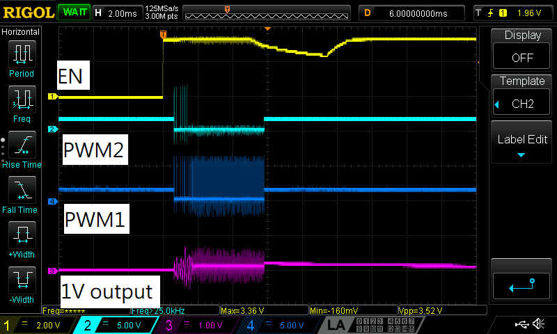
When I apply the enable signal to TPS40428+CSD95378B, the system cannot provide 1V output in 1 go.

As I see it usually cause large current in the first time (12V input drop to 9V) and undergo a few restart before output stay on 1V.

Tracing back I found 1 of the PWM signal stay idle when powering up...

Can we get any hints from below waveform?

  • Hi Alex, 

    What are your specs for this device? It looks like two phase mode.
    What is your output current?

    Best,
    Ryan

  • My design reference from PMP9444, 

    12V input to 1V,40A output power a Xilinx Ultrascale FPGA

    560uF - EEF-GX0D561L

    100uF - TCJD107M016R0050E

    47uF - GRM32ER71A476KE15L

    22uF - GRM32ER71C226KE15L

    Thanks.

    TPS40428_sch.pdf

  • Since this error is happen by chance or say system instable, I have re-work on the loop circuit value

    but it not helping, the above waveform still happen by chance. (e.g. 2~3 times out of 10 enabling)

    Here is my loop calculation table

    7206.TPS40428 loop calculation_20230614_v2_man_2.xls

  • Hi Alex, 

    The schematic looks okay to me. Even in the top waveform it looks like the output should jump to 1 V instead of ramping like that. 

    Can you also include a waveform of VIN and PG?

    Best,
    Ryan

  • Hi Ryan,

    My board have some modification for now, pin PG1 is in NC state and cannot be probed.

    Below are waveform of VIN if success and if instable

    As I see the 12V Vin pull-down to 9V, trigger my 3.3V supply turn off and resetting sequencer/ EN signal


    Thanks,

    Alex.

  • Hi Alex, 
    I will get back to you tomorrow. 

    Best,
    Ryan

  • Hi Alex, 

    Perhaps it is due to your layout, are you able to send it? From the schematic it looks like everything is connected properly. Is Vdd for the power stage also dropping too when this happens?

    Best,
    Ryan

  • Hi Ryan,

    It will take me some time on the layout. Meanwhile can you help on review the loop calculation?

    Because I using this circuit to power up a FPGA, there are number of MLCC cap on FPGA side (0.22u~330uF) and I am not sure should they included in the calculation...

    Thanks,

    Alex.

  • Hi Alex,

    I looked at the calculations and they looked fine. If the FPGA side does have MLCCs too then you should include them. 

    Does this only happen with one device? Have you tried swap with a different part?

    Best,
    Ryan

  • Hi Ryan,

    If those MLCCs matter, is there any other tools table / app. note can help on calculate the compensation circuit value?

    Since TPS40k loop calculation table only have 1 type of output MLCCs slot

    I have 3 boards and have similar symptom that circuit may not boot up in 1 try.

    I know there is a design fault that pin 29,30 shorted and pin29 is desoldered in my board now, PG1 pin is NC.

    Thanks,

    Alex.

  • Hi Alex,

    After looking at the design fault has the issue changed at all?
    I would also check to see if the other signals are okay, enable, vref, vdd, vdrv. I would also check to see if the impedance between vin and gnd has dropped. 

    Best,

    Ryan

  • Hi Ryan,

    Yes, all my 3 board had touch-up fix by desolder pin29. ISH net is connected with 10k ohm in series only.

    I have EN, VIN captured on above posts, but no sure what is Vref, Vdrv you are metioning.

    And I do not think I have the equipment to measure impedance between Vin and Gnd...

    Anyway, I have captured some wave on FB and COMP net when device boot-up success or fail in below.


    Thanks,

    Alex.

  • Hi Alex, 

    There should be VDD and VDRV on the power stages?
    What faults are you seeing on the GUI? How many boards are you seeing this issue? Is it 2/10 for one board or across many boards?
    Best,

    Ryan

  • Hi Ryan,

    Do you mean the Vin pin and VDD pin of CSD95378B ?

    I use my System main 12V and a 5V buck converter feed to these pins and below are the captured waveform both success or fail boot up.

    As I can see the Supply volatge stay still most of the time.

    "OCF" "OCFW" may pop on GUI software.

    I got 3 boards and all have similar symptoms that device may need sending EN signal few times before giving stable output.


    Thanks,

    Alex.

  • Hi Alex,  

    What is your start-up / power on sequence? There is a startup sequence on page 21 of the datasheet. Ensure that you start up vin, operation/control pin, enable.

    Best,
    Ryan

  • Hi Ryan,

    I have configed the device start-up by send "EN" signal ("EN" high on pin3 "CNTL1).

    SS time = 9ms

    Everytime i start-up the devcie I have provide a stable 12V and 5V before sending EN high

    and per DS the ton(dly) is 0ms in defalut setting, and I can't find any other description about minimum turn-on delay time.

    By the way, any idea of why "COMP" can drive up to ~3.3V during start-up ?

    Thanks,

    Alex.

  • Hi Alex, 

    The COMP pin is meant so that all of the phases to share the same voltage. The current sensed from each phase is compared to this and then fed into comp. Depending on the error, the PWM is generated. I believe it is that high because the output was not increasing so the COMP pin voltage increased in order to ramp up the PWM to increase the output. However, it should not be going that high, normally would be around 1.5 V.

    Best,
    Ryan

  • Hi Ryan,

    Another question, Do pin 29 "PG1" floating will cause any error detection and feedback to PWM logic?

    Or do bad GND plane placement will cause IC need longer feedback time?

    (e.g. Comp. circuit reference to PGND not AGND

    Or Voltage/Current feedback reference to noise Digital GND)

    Thanks,

    Alex.

  • Hi Alex,

    A few questions:

    1. What is the peak VIN current value in this image?

    2. Would it be possible to get a closer look at the PWM signals during the start-up transient? Instability should be visible in the PWM line as a rapidly changing duty cycle. A shot like the one below (previously in this thread) but with EN replaced with 12VIN & further zoomed in so individual PWM pulses could be seen could be useful in confirming this is a stability issue.

    I'll look more into the math model for your compensation loop to see if changes need to be made from a theory standpoint.

    Thanks,

    Travis

  • Hi Alex,

    I read through and understood the problem is intermittent. Does the board stay on when the problem occurs? Is there any load connected to the output? Can you please measure the loop across R66 when the board is on?

    Regards

  • Hi Sir,

    And by reviewing my setup I think I have used a bad conductivity power cord which have ~1V drop. By changing the power cord I cannot see the 12Vin input drop anymore, but still I found 3 types of output fail symptoms.

    the power sequencer can re-generate "EN" few times, so eventually the whole circuit can provide stable 1V output. But I afraid this is a potneial risk of my systme.

    1. I have re-measure the in-rush current and it is up to ~1.6A on 12V input.

    2. I have try capturing the PWM signal in attached excel, hope you can get enough hints from that.

    3. Yes, I got a FPGA and its CAP as a load of the circuit.

    waveform of "DIFFO" and across "R66" also in attached excel 

    Thanks,

    Alex.

    VCCINT_fail_symptoms.xlsx 

  • Hi Alex, 

    I think the board has excessive output capacitance. Can you please remove the 560uF and try?

    Regards

  • Hi Mahmoud,

    Since my board is quite large and hard to remove a cap, destructive touch-up will be my last option.

    Because my design reference from PMP9444 and it already have the 560uF in schematic, I do not it will be the issue...

    Best Regards,

    Alex.

  • Hi Alex,

    It looks like there is an over current at power up. This is why I thought about excessive capacitance. How about the inductor rated current?

    Regards