This thread has been locked.

If you have a related question, please click the "Ask a related question" button in the top right corner. The newly created question will be automatically linked to this question.

BQ76952: BQ76952 shutdown/reset or just doesn't run while high load discharging

Part Number: BQ76952


Hi TI Team,

We designed bms with bq76952 and we already used this bms under these conditions:

100A continuous discharge with 14 parallel fet(7 charge and 7 discharge, these mosfets specs are; gate charge 210nc @ 10v and Vgs 4.5V @ 250µA )   

If we talk about on TI Multiple FETs with the BQ769x2 Battery Monitors Application Note, our gate resistors(r4,r5,r6..-r1,r2,r3..) is same with this application notes value 51 ohm and also our R44 is 1k to our R45+R40 total resistance is 57k and R41 is 1K  this circuit works fine under 200A discharge(10s-15s),

However, when we use 16 parallel fet(8 charge and 8 discharge, these mosfets specs are; gate charge 210nc @ 10v and Vgs 3.8V @ 270µA ) but in this situation we can't open fets over 120A discharge current and I2C communication fail at this time.

if we start the load with 100A and increase the current to 150 or 200A while the load turn on, FET was still open but when we start the load with over 120A, FET was turn off.

We tried these solutions;

First, we think problem will occur because of the CP1 capacitance then we increase both the CP1 and BAT capacitance 1uf and try it. We repeat the same steps until both capacitances reached 18uf but nothing changed

Second, we increase R45+R40 and R1 the decrease these resistors values different level but nothing change

Third, we remove the D7. The closing problem doesn't happen so we turn-off the FETs over R45+R40(56K) and this mean our turn-off time get long, this create two different problems. First problem is turn-off time too long for SCD protection and second problem is mosfet drived at linear region to long and fets crush at scd.

Fourth, we decrease R45+R40 1K ohm while D7 is removed. It still can't turn-on until R45+R40 total resistance increase to 33k but the result almost the same as the third step.

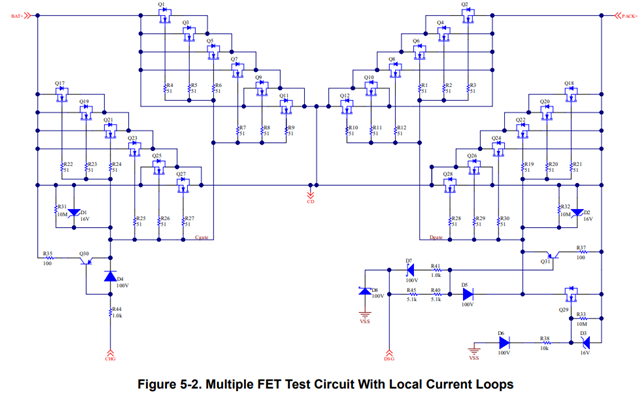
This picture shows the voltage on the shunt resistor when trying 150A discharge but fet problem occurs in that instance.   

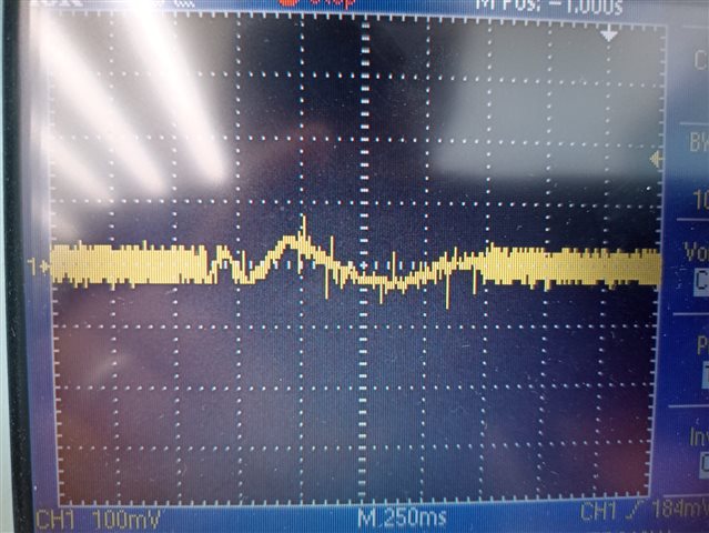
The second picture shows the Vgs voltage of the fets when trying 150A discharge but the fet problem occurs in that instance.   

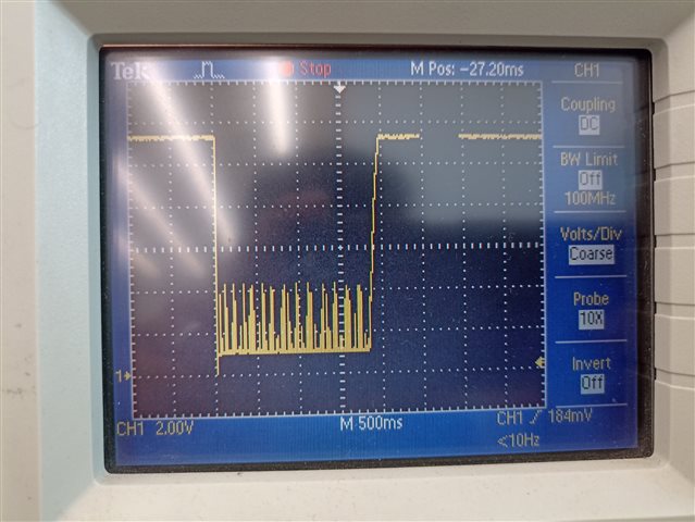
thirth picture shows CP1 voltage during same stiuation 

Thanks in advance,

Canberk

  • Hello Canberk,

    The Charge pump only has an effect on turning-ON the FETs. I believe your concern is more about the turn OFF. 

    Have you tried decreasing the gate resistance for each individual parallel FETs? The turn-off might be too slow. I suggest to probe the turn-off response at each one of the parallel FETs and see if it happens in all of them or if it's a specific FET not turning off. Usually it is the last FET the affected one. You can reference to this FAQ where good information is mentioned about Parallel FETs oscillating during turn off.

    As mentioned in the multiple parallel FETs app note, "When the diode drop across D4 and D5 is a concern a Schottky type diode could be used or a large value parallel resistor may be added to bring the gates to full voltage after the initial current surge". This might be useful for the turn ON. 

    Regards,
    Jose Couso

  • Hello Jose,

    As I mentioned "Second, we increase R45+R40 and R1 the decrease these resistors values different level but nothing change" part ı tried that. As I explained above, the turn-off of the fets happens too slowly it's not a debate. Our problem is when we decrease these resistors 952 gonna be shut down and I2C communication will fail, However, if we increase these resistors also as I mentioned above "turn-off time too long for SCD protection and the second problem is mosfet driven at the linear region to long and fets crush at SCD."

    Thanks for your reply

    Regards,

  • Hello Canberk,

    From the pictures shared above, it can be seeing that some sort of leakage is happening at the DSG and CHG pins affecting the charge pump voltage.

    Please share your schematic to further assist you.

    Regards,
    Jose Couso

  • Hi Jose,

    I send the schematic through a private message, there is a small difference in a real PCB, DSG gate resistors are 100ohm(instead of 150)

    Regards.

  • Hello Canberk,

    The schematic looks fine. Nothing alarming in the DSG and CHG paths.

    Can you please have different scope channels. One for SRP and SRN, one for the DSG or CHG gate, and one for the charge pump for when this occur? The pictures above do not look synchronized and it is hard to debug this way.

    From the pictures above, it does seem the part recovers itself. You mentioned the device loses communication, does communication recover by itself?

    One thing I noted from the schematic is the TS2 connection. The TS2 pin should be left floating if shutdown is intended to be used. I see it is connected to a BMS_BOOT signal which I do not know where this goes. Also, how do you reset the part? 

    Regards,
    Jose Couso

  • Hi Jose,

    Firstly ı click "This resolved my issue " button wrongly our problem is still the same, we get a synchronized oscilloscope screenshot today, but

    second communication recover itself.

    and BMS_BOOT pin (TS2_PİN) connect to MCU we will remove this path and try again.