This thread has been locked.

If you have a related question, please click the "Ask a related question" button in the top right corner. The newly created question will be automatically linked to this question.

TPS55165-Q1: not 12V out

Part Number: TPS55165-Q1

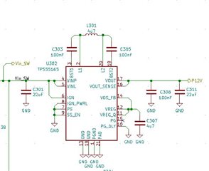
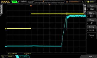
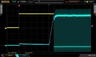
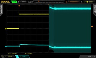
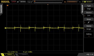
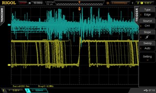
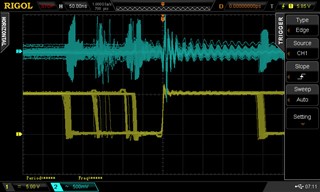
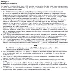
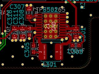
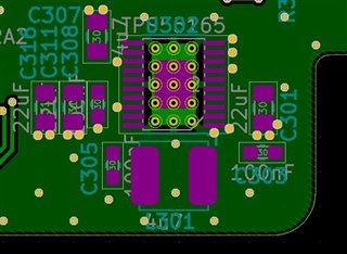
I have made a design per the webench recommendation to generate 12V out. Input is from a 3 cell Li Ion battery.  Nominal 10.6V.  Output measures 8.7 in one instance, 9 V in a second instance of the circuit no load.  Vref measures 4.89V and connects to Vos_fb to output 12V.  Why isn't it 12V?

  • Hi Jan,

    1. Could you reply with the schematic and layout?

    2. Could you also share with the waveforms you have captured like Vin, Vout, SW1, SW2, iL?

    Regards,

    Bryce

  • I don't have any waveforms captured, but will do so.

    I have screen shots of the relevant parts of the schematic and layout but I'm uncertain how to include them here.  The schematic matches the results of WEBENCH with Vin 9 to 12V6, Vout 12V, 0.25A

  • The layout.  Pin 1 lower right.  top and bottom ground planes stitched together

  • Some of the requested waveforms.  It is noted that the input voltage is 12.2V and DC output is 9.9V.  Earlier measurements were taken with Vin about 10.6V and Vout  just under 9V.

    Waveform is consistent with simulation except that the output does not reach 12V. Yellow trace is Vin. Blue trace is Vout

    waveform at L2, pin 20, at startup

    waveform at L1, pin 2, at startup

    All measurements taken with no load

  • Hi Jan,

    Could you check the chip that you are using is TPS55165-Q1, not TPS55160 or TPS55162? The three parts Vout configuration is different.

    I could see there is no big problem with the schematic.

    But the layout has big difference with TI recommendation. For DC/DC converter, we saw more than 50% of issue is related to the layout. For example, the power trace (PCB trace between Cin, Cout, inductor to IC power pins) should be wide enough. 

    Are you pretty sure that the waveform is test at no load condition? 

  • Thank you for your response.  The markings on the IC are TPS55165, 35TG4, A2VL. I am sure the waveforms are with no load. The two 12V loads are externally connected to the PCB and they were not connected during the test. Even when they are connected they draw well under 100mA, which shouldn't be anywhere close to taxing the TPS55165.

  • Hi Jan,

    Thank you for your confirmation. 

    What's the inductor saturation current level? 

    I think you could some test to debug:

    1. Replace a new chip on the board, see if Vout is same.

    2. Probe VREG pin waveform. The VREG pin is supply of internal circuit and needs to be correct first.

    3. Connect VOS_FB pin to GND, check if VOUT is 5V or not.

    I'm still suspecting the issue is related to layout.

  • The inductor is a TDK VLS5045EX-4R7M, 36 milliohm, Isat 4.4A.

    I have two units constructed. Both have the same problem so I highly doubt that changing the part will help so I respectfully decline to do that.

    Unit 1 Vin: 12V21.  Vout: 9v91  Vreg: 4V89

    Unit 2 Vin:12V21  Vout: 9V78  Vreg: 4V93

    I will modify one by cutting the trace to VOS_FB and grounding the pin and I will put a scope on Vreg to make sure it is behaving.  What should I see on that pin other than a DC level?

  • Unit 2 modified to output 5V (pin 4 grounded).  Output 5V04 no load.  Vreg 4V88.

    I put a scope on the Vreg output.

    AC coupled, spikes at switching less than 100mV peak to peak.

    If this is a layout problem what changes do you suggest? The caps on Vin and Vout are about as close to the IC as I can get and tie to a ground plane.

  • Hi Jan,

    The inductor is fine.

    When VOS_FB is short to GND, the Vout should be 5V and your test result matches with expectation.

    What's the output capacitor Part number? Comparing with EVM, the selected capacitor size is much smaller, I'm suspecting the effective capacitor value is much smaller. may cause loop instablility.

    You can probe inductor current as well and zoom in the switching waveform, check if duty cycle changes cycle by cycle.

  • Hi Zack,

    We're in agreement regarding the 5V result. I assume that the Vref node is working as expected.  There are two caps in parallel for the output.  C308 is 100nF, 50V, X7R.  C311 is a 22uF, 25V, X5R.  I'll reconnect for 12V out and probe L1 and L2 nodes.  My hunch is that the part is not transitioning from buck to boost, but I sure don't know why.  Would it be reasonable to use a bench supply instead of the battery and see what happens driving it with 9V?

  • Some interesting numbers using a bench supply for Vin.  All taken with no load.

    Vin 8V52  Vout: 9V01

    Vin: 9V01  Vout: 9V14

    Vin: 9V5  Vout: 9V31

    Vin: 10V0  Vout:  9V29

    Vin: 10V5  Vout: 9V18

    Vin: 11V01  Vout: 8V9

  • Any response updates?  In the intended application the loads are modest and are switched on and off as necessary so behavior at no load is important.

  • I just tried doubling the output capacitance to 44uF by piggybacking a second 22uF on top of the first one (C311).  It makes no difference.

  • Hi Jan,

    Sorry we were on public holidays on last days.

    Could you probe the waveforms of inductor current, L1, L2 and Vout at one page? So that we can check the waveforms cycle by cycle.

    Regards,

    Bryce

  • Hello Bryce,

    I only have access to a 2 channel scope and I don't have a means to look at the inductor current.  I can, and will, take waveforms of L1 and Vout and then L2 and Vout.

  • Here are the waveforms taken.  Vout is blue trace, AC coupled.  L1/L2 is yellow trace, DC coupled.  Sweep speed 50nS/div. Ch1(yellow) 5v/div. Ch2 (blue) 500mV/div

    L1, Vout

    Typical L1, Vout single shot

    L2, Vout

    L2, Vout single shot

  • Hi Jan,

    Thanks for your waveforms, could you put the inductor upright and add a line between the inductor pad and the PCB pad like below, so that you can capture the current waveform with a current probe? I can not see anything abnormal from the above waveforms, can you zoom out and capture the iL and L1 or L2 around 10-20 switching cycles in the scope?

    Regards,

    Bryce

  • Hi Bryce,

    I don't have access to a current probe so trying to modify the board is a moot suggestion. I will recapture L1 and L2.

  • Hi Jan,

    Thanks, please reply on this thread when you get results.

  • Here's L1 at 500nS per division

    and both L2 (yellow trace) and L1(blue).  Same sweep speed

  • Hi Jan,

    It looks like the device operation is unstable.

    Can you add another 22uF output cap at the output side and test again?

    I don't see any copper planes on the layout, does it have polygon planes actually?

    Regards,

    Bryce

  • Hi Bryce,

    It already has an extra 22uF on the output piggybacked on the first one.  In fact, there are copper ground planes on both layers and it's pretty continuous on the bottom (green) layer.  The only layout related issue that may exist is that the ground side of both input and output caps are not as close to pin 1 as they could be.  I have made a change to reorient them and expect to have the bare boards next week to test it out.

  • Hi Jan,

    Yes, what is the part number of the output 22uF you used? The capacitance value could derate a lot due to dc bias. I am wondering if it could help when you add more caps.

    Also, the layout could do great impact on the operation. Looking forward to your results.

    Regards,

    Bryce

  • Hello Bryce,

    The 22uF caps are Samsung CL21A226MAYNNNE.  25V, X5R.  I am aware of the cap degrading when subject to DC bias, as these are.  That happens to be why I chose parts rated at more than twice their expected working voltage.

  • Hi Jan,

    It makes sense considering the dc bias when selecting MLCC caps.

    Looking forward to your results Slight smile

  • Initial testing of the revised layout is virtually the  same as before.  Two units built up and tested.

    Vin: 12.15V

    Unit 1 Vout, no load:  9.03V

    Unit 2 Vout, no load: 10.42V

    Both units have 44uF on the output (2x22uF).

    I will take scope pictures of L1 and L2

  • Here are  the waveforms for L1 and L2 from the revised layout boards.

    unit 1

    yellow trace L1, blue trace L2.  Shows the same instability as  the old layout.

    unit 2

    yellow trace L1, blue trace L2. It is noted that while the output starts at 10.4V after a few minutes and probing the inductor pads that the output is 12.03V and these waveforms have stabilized, as shown.  My continuing concern  is the lack of repeatability from one instance to the next and the apparent minimal margin of stability.  As noted earlier the application requires a valid level at no load.

  • Hi Jan,

    It also confuses me that the waveforms get stabilized when you add the probe at L1, L2. 

    I searched the output cap, and found that the effective value is only 20% at 12Vdc, what about if you add up to 22uF effective value?

    What is the part number of the inductor? Would it help if you rotate the inductor?

    Regards,

    Bryce

  • As stated earlier, the inductor is a TDK VLS5045EX-4R7M.  4.7uH  Isat 4.4A  36 milliohms.  Rotating it will only complicate the layout by putting the pads perpendicular to the long axis of the IC,  There is already two 22uF caps in parallel on the output on both boards.  All I can tell you about behavior of board #2 is that the output voltage is closer to the intended value on power up and the L1 and L2 waveforms are stable when probed.  Board #1 is the same layout and components but does not get as close to the intended output nor do the  waveforms stabilize.

  • HI Jan,

    Yes, understanding that. But the device is unstable now, so I think you can take the actions recommended above to have a try. 

    I mean the inductor can rotate 180° the layout would not change.

    The 22uF is the rated value, the effective value would decrease a lot due to dc bias.

    Regards,

    Bryce

  • In the course of rotating the inductor the TPS55165 was destroyed.  After replacing it with a different one the output voltage is 10.3V.  Then I added a third 22uF to the output.  No change in output.

    I have to state that I don't understand why rotating the inductor would make any difference.  It is a 2 terminal device and rotating it 180 degrees  shouldn't matter.  The windings and core still have the same relationship to the traces and the ic.

  • Hi Jan,

    After rotating the inductor, the internal winding of the inductor which is on high-side or low-side of the inductor changes, and the area of the high frequency switching node could increase which may introduce more interference. But I am not sure if this can damage the device. I prefer to think that the poor layout caused damage. As mentioned above, the layout has big difference with TI recommendation. For DC/DC converter, we saw more than 50% of issue is related to the layout. For example, the power trace (PCB trace between Cin, Cout, inductor to IC power pins) should be wide enough. 

  • To clarify, rotation of the inductor did not cause damage to the TPS55165.  In the course of heating the area up it shifted relative to the pcb land pattern.  I didn't notice that until the magic smoke escaped. When I redid the layout I doubled up on the vias to connect pin 1 to the ground plane and I oriented the input and output caps to minimize the distances to pin 1 and minimize the input and output loop area per the TI application information.  At this point I don't know what can be done to make this circuit stable and reliable enough to commit to a product.

  • Hi Jan,

    I am not sure, does the heating cause damage to the pad so the device get damaged?

    You can follow the TI recommended layout and share your file so we can review it for you.

  • The pad didn't get damaged.  In fact, the TPS55165 moved a bit when the solder was melted to rotate the inductor.  I consider this totally the fault of the technician (me).

    I have followed the example circuit layout and explanation to the best of my ability.  If anything the input and output capacitors are located closer than the recommended layout with the IC ground pad pin 1, and the capacitor ground sides all tied to a ground plane with no intervening traces.

  • Hi Jan,

    Understand, there maybe some pins were wrong connected which cause damage.

    Could you share your revised layout so I can review it?

  • Here is the current layout

    red traces top side. Copper pours shown in outline form. Top and bottom copper pours connected to ground.

    Here's the bottom side filled, top side hidden

  • Hi Jan,

    I have been following this thread from quite a while now. It can be frustrating to find that after all the intricate details you go through the design still doesn't work as intended. I have had a similar issue where the output voltage wasn't stable and later on I fixed it by correcting my layout design. So I can tell you that the issue you have may well be coming from the layout design.

    Thanks!

    Khan

  • Thank you for your message Kahn.  I've been using KiCad for more than 10 years now both professionally and personally.  I've done the layout according to the principles set forth by TI as well as what I've learned over the years.  Minimize the loop area of the switching paths.  Keep the ground connections as close as you can and don't cut into them, for example.  I'm more than willing to revise the layout IF there is something specific identified.

  • Jan,

    Now that I think about the problem and look at your layout design in detail I have had exactly the same problem in my buck converter design. You see the VOUT_SENSE pin connection in your layout, it is not supposed to be connected directly to the VOUT pin it has to be connected after all the output capacitors. Like I showed in the picture below. I know it is the same node and normally it shouldn't matter where you connect a trace on that node but in this case, VOUT_SENSE is working as feedback to control the output voltage so it has to come from the capacitor. Try this and I bet it will work 100%.

    If you want to try it before you change the layout and order PCBs which is a hassle and could potentially take another week or more. Lift pin 16 up until it disconnects from the footprint then solder a jumper wire from the pin to the last output capacitor C316. It will take a bit of soldering gymnastics but it will be fun. Follow this tutorial if you need to, https://www.sparkfun.com/tutorials/99, they explained it quite well.

    Thanks!

    Khan

  • Hello Khan,

    I was able to cut the connection between pins 16 and 17 without breaking the pin 17 to output. And I added a wire  from pin 16 to the output cap at C316. This is a board that powered up with an output of 10.3V.  After the modification, it powers up to 12.03V.  Right on the mark. I think your suggestion has solved the issue.  I'll make the mod to a second board to confirm and then make a minimal change to the layout to match the kludge.  

    Thank you.

  • Second board modified.  Second board is working as it is supposed to.  Problem solved.  Layout has been changed.