This thread has been locked.

If you have a related question, please click the "Ask a related question" button in the top right corner. The newly created question will be automatically linked to this question.

TLV700: Vout>Vin+0.3V

Part Number: TLV700

Hi,

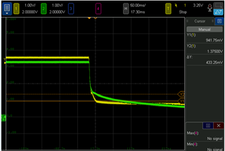
Currently we are using TLV70033 in our design. During power down, there is a small moment (<100ms) where the Vout>Vin by ~0.45V as below.

Question: Will the LDO damage if Vout>Vin+0.3V for such short period of time? Please advise.

Vin=yellow, Vout=green.

  • Hi,

    How much output cap do you have? 100ms isn't actually very short, but this is actually a good thing here because the reverse current is probably pretty small since the shutdown takes so long. Unless you have a very large output cap, I don't expect this to cause issues. Something to keep in mind is that the device may have weird behavior if it is powered up again before the input goes all the way to 0V after it has had a small reverse voltage. 

    Regards,

    Nick

  • May i know what is the weird behavior that we should anticipate?

    We are using 2x TLV70033 and each has approximately 30uF and 70uF at the load side. We tried having a pull down resistor of 100kOhm at the output of the LDO but not really helping much. 

    We have PCB constraint and adding diode in between output and input may not be possible. 

  • Hi,

    The behavior I was referring to is mostly some sort of latching behavior. The manifestation of it would be that the device still turns on and regulates, but the regulation point could be a different set point. 

    It makes sense that a 100k pull-down resistor does not help because the time constant for 70uF and 100k is 7 seconds. You would need a resistor closer to 150ohm to realistically help prevent the reverse voltage, but that adds around 20mA load to the device. 

    Regards,

    Nick

  • Hi,

    May i know what is the forward voltage for the internal body diode of this LDO?

  • Hi,

    The body diode normally starts conducting at around 400mV or so. This is why the abs max spec for VOUT is normally VIN + 0.3V (going beyond 300mV starts to get into the region where the body diode can begin conducting). 

    Regards,

    Nick

  • Thanks for the info. 

    I have further few questions:

    - based on calculation, the reverse current is approximately 10mA based on the Cdv/dt calculation. Can i say that this amount of current is low risk?

    - what is the exact parameter value that will trigger latch on LDO? According to TI white paper SCAA124 on latch up, it states that as long as not exceeding the absolute maximum rating, latch up is not a risk. 

  • Hi,

    Yes I think the risk of damage from the conditions you are seeing is low. The risk of latching increases the further you go from the abs max rating. I can't provide the exact parameter value that triggers latching because it is different for every device. The reverse current is the parameter of concern; the latching is caused by the reverse current charging internal nets and causing the control loop to behave in unexpected ways. If the device input is allowed to settle all the way to 0V, the latching condition is removed since the internal nets can be discharged. 

    Regards,

    Nick