This thread has been locked.

If you have a related question, please click the "Ask a related question" button in the top right corner. The newly created question will be automatically linked to this question.

LM74900Q1EVM: modified below schematic to achieve Vin= 40V – 62V

Part Number: LM74900Q1EVM

Dear Taru,


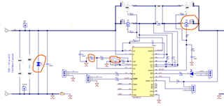
I have modified below schematic to achieve Vin= 40V – 62V and changed the following components values


  1. R14= 1K, R16= 1.65V according to give formula in datasheet.
  2. Removed D1 TVS diode.

But when I am powering up the board MOSFET Q4 immediately damaged.

Then I have also changed this Q4 MOSFET with NTMFS015N10MCLT1G but again it damaged.

Need your advice.  

  • Hi Vipin,

    Looks like the FET SOA is being violated while starting up with output capactior.

    To prove the above point you can remove the output capacitance and try powering up the EVM. The FET should not get damaged with startup into no capacitance and no load.

    Next you can use the attached design calculator to check if the FET selected has enough SOA margin while staring up for a particular Vin(max) and output capacitance. You may have to increase the Cdvdt to obtain good FET margin.

    Please go through the training videos (click on the links provided in the design calculator)  before using the design calculator. 

    5086.LM749X0_ID_Design_Calculator.XLSX