This thread has been locked.

If you have a related question, please click the "Ask a related question" button in the top right corner. The newly created question will be automatically linked to this question.

TPS23754: EMI; switching waveforms

Part Number: TPS23754
Other Parts Discussed in Thread: TPS23734EVM-094, TPS23756EVM, , PMP10288, PMP9563

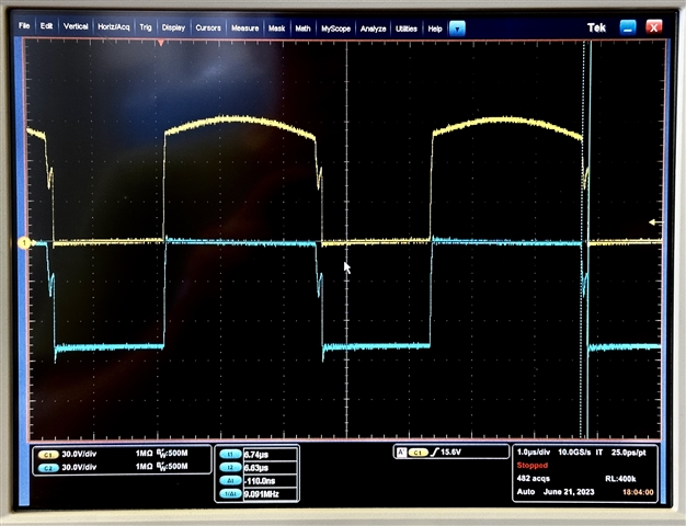
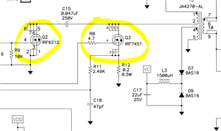
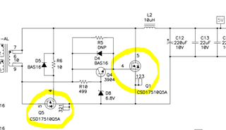
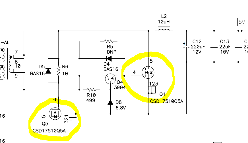
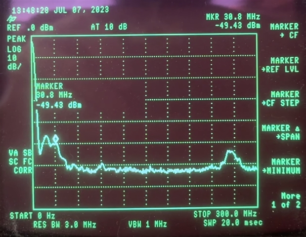
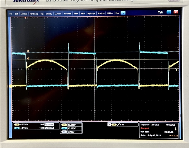
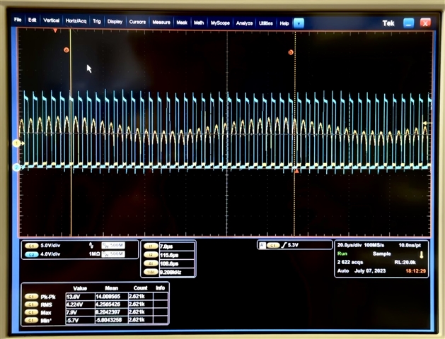
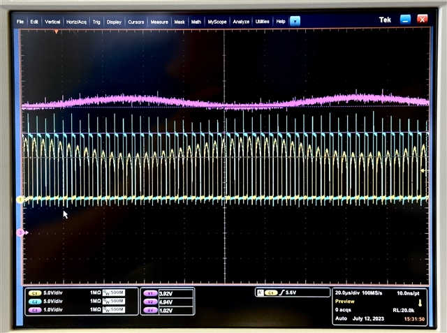
I designed our board based on the PMP5818 ACF design. It works, but am having trouble with EMI in the 30-50 MHz range. I've attached a scope trace of the waveforms for the main switching and clamp transistors. There doesn't appear to be any ringing that would be likely to cause 30 MHz EMI. Except possibly for that glitch on the falling edge of the waveforms. Are these waveforms you would expect on this design?

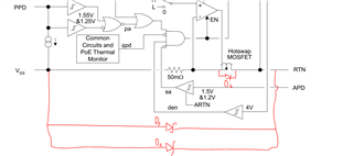
Also, none of the ACF reference designs that I've looked at on the TI website use snubbers on the main switching and clamp transistors. Are they of any use on these transistors?

Thanks

  • Hi David,

    Thanks for reaching out!

    Do you have any adapters connected during the EMI test? The PD switching frequency is ~ 250 kHz, and normally itself can hardly cause high magnitude EMI at 30-50MHz.

    The below application note may help to solve EMI issue:

    www.ti.com/.../slua454.pdf

    Best regards,

    Diang

  • Hi Diang,

    This is an isolated design, and I have seen a similar app note for isolated designs slua469.

    Checking the board with a sniffer probe, the hottest point on the board is the transformer, and the spectrum below 50 MHz is quite pronounced.

    Thanks,

    David

  • Hi David,

    Thanks for the additional information.

    Do your mean the DC/DC converter transformer or the data transformer? 

    I sometimes saw the highest space noise is near the DC/DC converter transformer, but it should be the same with the switching frequency. While, there could be some higher order harmonics but should be very low amplitude at x0 MHz range.

    Adding chokes and beads are useful ways in many cases to reduce the EMI amplitude. Besides, may I know where is your bob-smith ground connected with? 

    Best regards,

    Diang

  • I meant the DC/DC converter transformer. 

    The Bob Smith ground is connected at a single point to the board main ground, on the opposite side of the RJ45 from the PoE supply.

    I use two ferrite beads at the input to the PoE supply from the Ethernet bridge, as is shown in the PMP5818 design.

    BTW, forgot to answer your previous question: for EMI testing, as well as normal operation, the board is connected only to Ethernet and an iPad via a USBC cable.

    Thanks,

    David

  • Hi David,

    Thanks for your additional information. 

    In your voltage waveform, looks like they are the Drain/Source voltage of Q3 and Q2.  

    The turn off voltage of these two MOSFETs V_off = Vin/(1-D). In your case, it is about 80 - 90V, while you have a D = ~45%. This gives a ~47 V input voltage, which is reasonable for PoE input voltage.   

    For the RC snubber circuit in parallel with the main FET (Q3), it may help to absorb the high order harmonics, but I think it may not change too much for EMI in the 30-50 MHz range since there is already a C15-Q2 circuit can do some of the snubber job to a certain extend.

    The secondary side FETs (Q4 and Q5) sometimes suffer a high voltage spike if without a snubber circuit. You can check whether they have such a spike which may cause EMI issue. TPS23734EVM can be a reference for secondary side snubber circuit design. www.ti.com/.../sluucb6a.pdf

    Best regards,

    Diang

  • Hi Diang,

    There were indeed some spikes on Q4 & Q5, and ringing. I added the recommended snubbers in the reference you gave me. Measuring the current on the cables with a cable clamp, there wasn't much change in the EMI spectrum (I have not tested in the test chamber yet). Low frequencies increased slightly (~1.0 dB), while higher frequencies decreased slightly more (~2.0 dB).

    If I understand you correctly, this circuit should not be producing EMI signals in the 30-50 MHz range.

    Could the layout be the cause of the signals? Here is the top side layout of the PoE section. Comparing with the layout in the TPS23754EVM, My layout of the primary switching circuit looks, if anything, tighter than the TPS23754EVM (connected to pins 1 & 2 of the transformer which is mostly off the page). The active clamp however is in the upper right corner, connected to the C62 cap. Could this be the cause? 

    The board is 6 layers, 2 internal RTN planes, with RTN plane fill on top and bottom. There are no components on the back side, only non-critical connecting traces, and also non-critical connecting traces on an internal layer.

    Thanks,

    David

  • Hi David,

    Thanks for your follow-up.

    Yes, I think PoE should not be a strong resource to generate 30-50 MHz EMI. It could be a strong source for 205 kHz (switching frequency) noise.

    While the high frequency EMI may pass through the PoE. If we could add some impedance in the EMI path, we still should be able to reduce the EMI. CM chokes and beads / fixed inductors could be tried to see if they cause any impacts on the EMI tests. 

    For the layout, I could see the switching node (red cycled) is large, which may cause some EMI issues since it has a relative large capacitance. You can try to increase the gate resistance of the primary FET to see if it cause any change for your EMI results.

    Best regards,

    Diang

  • Hi Diang,

    I tried increasing the gate resistors to the primary FET and the clamp FET from 4.7 ohm to 12 ohm. Didn't see any change in the spectra read from a cable clamp around the USBC cable. Based on the Ciss of the switching transistors, it looks like it would need to be about 100 ohms to affect anything.

    I will work on a new layout that will tighten up the loops. Do you want to hear the results once we've spun the board? How do I do that? Looks like you guys usually close the thread after a week or so.

    Thanks,

    David

  • Hi David,

    Thanks for your update.

    I do not know how much it can improve if redo the layout just for reducing the switching node area...

    I feel changing the decoupling capacitors or isolating capacitors (X, Y caps), or adjusting inductors make more effects in EMI test in most cases.

    You can reply or open a new thread if the old thread is closed.

    Best regards,

    Diang

  • Hi Diana,

    I bought a TPS23754EVM-383. Using a cable clamp probe on both the Ethernet input and the 12V output, I compared the spectra of the TPS23754EVM-383 with the spectra of our board. At 30 MHz, the spectra were virtually identical. This indicates that the design does produce frequencies in the 30 MHz band.

    Thanks,

    David

  • Hi David, 

    Diang is currently out of office and will return July 5th, thank you for your patience! 

    Thanks and Regards,
    Raymond Lin

  • Hi David, 

    Thanks for your test.

    Could your do a control test if you have other dc/dc converter with 20-50 W power and 100 - 500 kHz switching frequency?

    I would suspect there is some 30-MHz noise source other than TPS23754EVM-383, but the TPS23754EVM-383 has the path for the noise. Inductors may help to reduce the noise amplitude if applicable.

    Best regards,

    Diang

  • Hi Diang,

    Please see attached document. The 30 MHz signals are related in magnitude to the amount of power output by the TPS23754EVM. Also, when the Ethernet cable is unplugged the noise floor is flat, with no sign of 30 MHz signals.

    I don't have a comparable device for testing other than our own board. The 30 MHz signals are almost identical between our board and the TPS23754EVM, using the same setup. The noise signals we see are also very similar to the ones seen when testing in an EMI 10 meter test chamber.

    "Inductors may help ..." Please elaborate on inductors, which ones? Values? Changes in value of the existing ones in the EVM and reference designs?

    Thanks,

    David

    Source of 30 MHz signals.pdf

  • Hi David,

    Thanks for the attached report. Your test results were documented very well!

    Sorry that I need consult some engineers to ask the potential cause of 30 MHz noise and get back to you later. 

    Best regards,

    Diang

  • Hi David,

    Besides, I am confused that when Ethernet was disconnected, the TPS23754EVM should not have power except by a DC adapter input. 

    And you also have noise when Ethernet cable was disconnected

    Just wondering will the E-load be the noise source and could you try with a fixed load resistor? 

    Best regards,

    Diang

  • Hi David,

    Thanks for your patience.

    Had consulted a senior PoE engineer.

    The 30-40 MHz EMI noise may come from the secondary side sync FETs. Since you already added snubber circuits at Q1 and Q5, could you show their Vds voltage?

    Besides, for your test method, may I know which standard you followed for the EMI test procedure? A LISN (line impedance stabilization network) may be needed for a valid EMI measurement. Please find attached LISN, and there is an RJ45 input and output connector.

    Best regards,

    Diang

  • Hi Diang,

    When the PoE is disconnected from the TPS23754EVM there is no power to the EVM. Therefore, the spectrum when the PoE Ethernet cable is disconnected represents the noise floor consisting of internal spectrum analyzer noise + any ambient signals picked up by the cable clamp probe. The large spike between 0 Hz and ~ 10 MHz is an artifact produced by the spectrum analyzer. It is always there, even when there is no input to the spectrum analyzer.

    I plugged a 10 ohm resistor into the output of the TPS23754EVM. The spectrum obtained from the Ethernet cable is quite similar to the one using the electronic load. See attached screenshot. The 30 MHz signal is still there.

    Thanks,

    David

  • Hi David,

    Got it. Thanks for your reply.

    Have you tied to add / adjust the snubber circuit at the secondary side 2 FETs?

    Best regards,

    Diang

  • Hi Diang,

    A LISN is used for conducted emissions in the frequency range 150 kHz to 30 MHz. Since our device is not powered from the AC mains, we are not required to test for conducted emissions. We do have to test for radiated emissions from 30 MHz to 1 GHz for FCC and EU requirements.

    The Vds voltages for Q1 and Q5 are shown below.

    There is another problem. I don't see it all the time. There is an approximately 8 kHz oscillation on the 5.0 V output of L2. It's about 350 mV peak to peak, sometimes 1/3 less, sometimes not present. The oscillation appears on the Vds waveform for Q5 as well. The second screenshot shows the oscillation on the Vds waveform for Q5. Can this oscillation be related to the optocoupler feedback circuit for the output voltage? I copied the optocoupler feedback circuit directly from the PMP5818 reference design. I note that the TPS23756EVM design has some different values for the components in the optocoupler feedback circuit, as does the TPS23734EVM-094. All 3 designs are 5V/5A ACF designs.

    Thanks,

    David

  • Hi Diang,

    I added snubbers to both Q1 and Q5. I used values I found in the TPS23734EVM. 4.7nF+5.6 ohms for Q1, and 1.0nF+5.6 ohms for Q5 (I didn't have 5.1 ohm resistors). 

    Thanks,

    David

  • Hi David,

    Thanks for the waveform. Yes I can see a low frequency oscillation here.

    It looks strange only Q5's Vdsoff has it while Q1's Vdsoff looks ok. 

    Ignoring overshoot: for Q5, Vdsoff = Vout/D, for Q1, Vdsoff = Vout/(1-D). So if either D or Vout changes, both Q1 and Q5 should have similar oscillation.

    In your case I may doubt if the probe for Q5 measurement refereed to a proper ground since we saw the turn on voltage of Q5 is negative. 

    If it is a real oscillation issue, to me it could be:

    - oscillation could come from closed control loop

    - oscillation could come from output load

    - oscillation could come form the input voltage (less likely)

    Best regards,

    Diang

  • Hi Diang,

    My bad. I had been using AC coupling on channel 1 to measure noise, and forgot to switch it back to DC coupled. The previous screen capture is correct, with both waveforms referred to the same ground point and both DC coupled.

    Do you have a reference for designing the closed control loop? As I noted before, I used the values on the PMP5818 schematic. The TPS23756EVM, which is essentially the same chip, uses quite different values. The TPS23734EVM uses the same values for most parts, with a couple of exceptions.

    Thanks,

    David

  • Hi David,

    Thanks for your updates.

    The AC coupling makes sense that ch1 has negative Vds. So there is no 8 kHz at Vout actually?

    These two pdfs have information for ACF closed control loop design:

    www.ti.com/.../slua535a.pdf

    www.ti.com/.../slua702.pdf

    Besides, we have the reference designs for TPS23754 with ACF topology:

    Reference PD Class Vout Iout
    PMP10288 TPS23754 4 3.3 7.2
    PMP9563 TPS23754 4 12 2.5
    PMP7452 TPS23754  4 3.3 7.6
    TPS23754EVM-383 TPS23754 4 12 2.5

    Best regards,

    Diang

  • Hi Diang,

    There is definitely 8-9 kHz at Vout, as this screenshot shows. Channels 1&2 (Q5-yellow & Q1-blue) are both ref to the same ground point on the screen. Channel 3 (pink) is the 5V supply and is referenced to a different ground point on the screen.

    Thanks for the references. I will look into them.

    As for the reference designs, none of them are 5V 5A output. Doesn't that affect the feedback loop?

    Thanks,

    David

  • Hi David,

    Thanks for the waveform. There could be a feedback trouble to cause the Vout unstable. 

    Yes, the output voltage, output capacitance, output current will influence the feedback.

    Best regards,

    Diang

  • Hi Diang,

    Two questions:

    1) Some of the EVMs or reference designs for this or related parts place a diode between VSS and RTN ground. The TPS23754EVM-383 uses an SMAJ58A; the TPS23734EVM uses a B2100-13-F; and the TPS23756EVM and PMP5818 leave it out. What is the function of the diode, and could it conceivably affect the EMI?

    2) All designs place a 2200 pF, 2kV cap across the isolation gap between RTN ground and the output ground. The TPS23734EVM adds a 2200 pF, 2kV cap from the T1 input (ie the rectified, filtered PoE input voltage) to the output ground. However in the latter design it is listed as DNP. Is this strictly for high voltage protection, or does it also have a noise reduction function?

    Thanks,

    David

  • Hi David,

    1) Between VSS-RTN, SMAJ58A is a TVS diode and B2100-13-F is a Schottky diode. Besides, there is an internal hotswap FET between VSS-RTN which has a body diode. This diode can be forward bias when adapter is used and PoE is turned off.

    The Schottky diode can offer a lower voltage between VSS and RTN which is better for the chip reference voltage at this condition. It can increase the IC's performance at this condition since most of voltage references refer the VSS which is better to be the lowest voltage (while when diode is forward bias, VSS voltage is higher than RTN).

    The Zener diode can protect the internal hotswap better for avoiding avalanche breakdown.

    Both diodes are not mandatory in most of design cases. 

    2) These caps are mainly for common-mode noise reduction function.

    Best regards,

    Diang

  • Hi David,

    I will close this thread for now. Please reply or open a new thread if you have further questions.

    Best regards,

    Diang