This thread has been locked.

If you have a related question, please click the "Ask a related question" button in the top right corner. The newly created question will be automatically linked to this question.

TPS566231: Output ripple is high at lower operating temperature conditions

Part Number: TPS566231

Hi,

We are using the device P/N : TPS566231PRQFR to realization below DC-DC Buck conversion

Vin : 3.3Vdc

Vout : 1.24V/2A

Ripple and Noise : 30mv pk-pk (maximum)

Operating Temperature : -40DegC to +85DegC

We have tested output ripple for Vout : 1.24V/ 2A load at different operating temperature conditions as below

@ +25DegC : Output Ripple 14mv pk-pk 

@ +85DegC : Output Ripple 7mv pk-pk

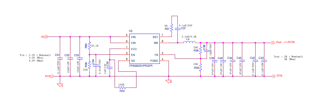
@ -10DegC : Output Ripple 79mv pk-pk

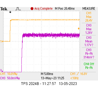
@ -20DegC : Output Ripple 84mv pk-pk

@ -40DegC : Output Ripple 64mv pk-pk

When regulator is testing at negative operating temperature i.e. -10DegC ,-20DegC & -40DegC output ripple is increasing drastically, however test setup, cable harness and measuring instruments are unchanged in all temp test conditions & regulator PCBA is conformal coated and fixed in sealed enclosure.

Regards

AM

  • Hi AM,

    The ripple increase does seem quite high. Can you please share your schematic, BOM for this design? And also is it possible to share the SW and VOUT waveforms when at room/high temp vs cold temp? 

    Also, what is the max VIN and IOUT for this application?

    Thanks,

    Amod

  • Hello Amod,

    Vout ripple more than 30mv pk-pk is not acceptable in our application,

    Vin voltage : 3.0V ( Min) , 3.3V ( Nominal) & 4.0V (Maximum)

    Iout : 2A ( Nominal) & 3A ( Maximum) @1.2V Vout

    attaching the schematic along with part values mentioned for each part used

    Vout :1.2V/2A waveform 

    @ +25DegC ( Room Temp)

    Pink : Vout :1.2V/2A

    @ -55 DegC ( Cold Temp)

    Pink : Vout :1.2V/2A

    Regards

    AM

  • Hi AM,

    Unfortunately, the schematic image is very low resolution and I am unable to see much. If possible, can you please share as an attachment or pdf. Also, for your Vin and Iout requirements, TPS566231 is probably oversized and we could recommend better solutions if you are open to changing at the moment.

    Given that, how are you measuring the Vout ripple? I would recommend measuring with a pigtail method directly across the output cap with 1Mohm high impedance termination to minimize the noise during measurement. Also, curious what CH1 waveform is? It is hard to see the ripple clearly since it is zoomed out. If possible, please take measurement and show about 5-10 cycles of output voltage ripple. You can see an example of pigtail method and a ripple waveform in Figure 2 here: https://e2e.ti.com/blogs_/b/powerhouse/posts/how-you-measure-your-ripple-can-make-you-or-break-you 

    Thanks,
    Amod

  • Hello Amod,

    Pls find the attached schematic along with used parts value mentioned,

    Actually presently max Iout requirement is 3A, however it can be increased till 6A as per requirements

    Pls confirm, you would like to see ripple voltage (AC Signal) at SW and VOUT waveforms when at room/high temp vs cold temp? 

    Regards

    Atul Mishra

    TPS566231_Schematic & BOM.pdf 

  • Hi Atul,

    Yes even with 6A max and VIN <= 4V there will be other options that we can recommend. Let me know if this is something you are interested in.

    Back to TPS566231- The schematic looks fine to me. I do not see anything obviously wrong here. Yes please check the SW and VOUT waveform at room/high temp vs cold temp using the pigtail technique and record 5-10 cycles when the output is steady using appropriate voltage division units so as to see the signals clearly.

    Thanks,

    Amod 

  • Hello Amod,

    Please find the attached excel sheet for SW and VOUT waveform plots at room/high temp ( @25DegC) vs cold temp (-20DegC) pertain to Vout : 1.2V/2A, Max Iout : 6A

    Kind Regards

    AMSW & Vout Plots.xlsx

  • Hi AM,

    Amod is out of office. I will check and get you back next Monday.

    Thanks,

    Nancy

  • Hi AM,

    1. From the schematic, why is there no soft start capacitor? Why do you add R23(100K) from SS pin to VCC? You need to cap a soft start cap from SS pin to GND.

    2. From your waveforms, it seems the output voltage was in oscillation due to SW pulse not even spread. Could you try following suggestions?

    a. Make sure 3.3Vin has enough supply current for TPS566231 output up to 3A or 6A. 

    b. Remove C38 (10pF), test low temp to see if it improves.

    c. Make sure output capacitors C39, C40, C44, C45 (47uF) are X7R or X6S material. X5R, Y5V, Z5U should not be used.

    d. Please send us the PCB layout if above suggestions do not solve your issue.

    Thanks,

    Nancy

  • AM,

    The symbol is not match with the part number, you should use TPS566231P with PG function, right? if so, the pull-high resistor connected with SS is ok.

    please follow Nancy's comments to check (especially for b/c/d items)

    And add one more comment, you may try to decrease inductor to 1uH to check if any improvement.

    Finally please share layout if all suggestions not effective.

    Yuchang