This thread has been locked.

If you have a related question, please click the "Ask a related question" button in the top right corner. The newly created question will be automatically linked to this question.

UCC28070: Cannot work with load

Part Number: UCC28070

Hi E2E,

Our customer is designing a 3kW charger by UCC28070.

It is used for VIN AC150V~280V input. The Duty-Cycle is setted 0.95 and the frequency is 61kHz.

We found that VIN gradually increases from AC 150V to AC 200V, the no-load output voltage is a constant value.

When the VIN gradually increases from AC 200V to 280V, the output no-load voltage also rises. At the same time, the temperature of R87 and R105 resistors will also rise significantly during the whole process.
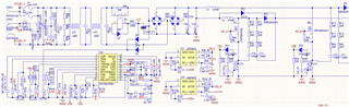
 

Then, We tried a load test with a 300Ω resistor. It cause the MOS to burn out. At this time, the current transformer detects that the current is infinite.

In this design, the Duty-Cycle of MOS conduction state is 0.95 , does it need to set the reverse? If so, how to configure the CSA and CSB?


  • Hi Tommy,

    Thank you for the query on UCC28070.

    There seems to be a number of issues in the schematic attached in terms of values of components. Specific to mention are the Rimo resistor, CT sense resistor, Rdmax resistor, voltage and current loop compensation which is causing duty cycle limitation as you load. I would advice to cross check with the calculations attached. Also please check the polarity of current transformers as the windings seems to be reversed in the schematic.

    UCC28070_calculations_review.pdf

    Please let us know your observations after making the changes and testing them.

    Regards,

    Harish

  • Hi Harish,

    We have carried out detailed design comparison and correction according to the PDF you gave before, but there are still a few points that we do not understand:

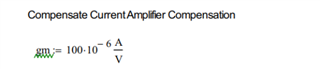
    1.What does gm and △Vea mean in the picture below? How to get a value?

    2. In the PDF page 13, there is another gm, What does gm mean ? How to get a value?

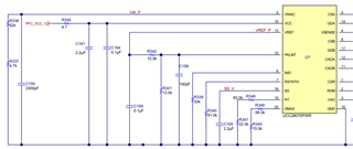
    3. In some reference design such as PMP40261. The VINAC(pin5)  the design uses a capacitor (C155), but it`s not use in DATASHEET.What should we treate VINAC?

  • Hi Tommy,

    These (gm) are fixed transconductance values of the internal current and voltage amplifiers. These are picked directly from datasheet.

    The Vea is the error amplifier output and it is limited at 3.2V.