This thread has been locked.

If you have a related question, please click the "Ask a related question" button in the top right corner. The newly created question will be automatically linked to this question.

TPS7A85A: TPS7A85A parallel design

Part Number: TPS7A85A
Other Parts Discussed in Thread: TPS7A85

Hello everyone,

I was pleased to see that the excel spreadsheet for calculating parallel LDOs has been updated with the addition of the TPS7A85A and the calculator for external resistors. Thank you! 

Now I would like to ask your help to verify the following desing:


1) In a previous thread (https://e2e.ti.com/support/power-management-group/power-management/f/power-management-forum/1189469/tps7a85-serial-vs-parallel-design-for-high-reliability)  TPS7A85A was recommended over the TPS7A85, but the TPS7A85A seems to have worse thermal characteristics...it's right? Did I miss something?

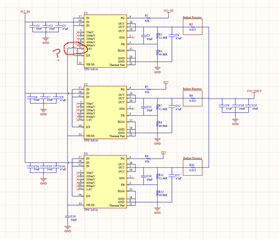
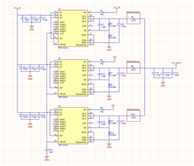
2) I connected all NR/SS pins together (like in TIDA-01232), is that correct?

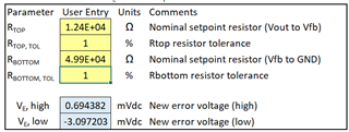
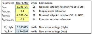
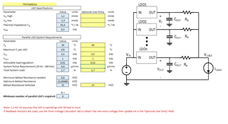
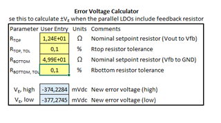
3) if I use external resistors calculator (with Rtop 12.4k and Rbot 49.9k, so Vout=1) i have Vₑ high = -374 and Vₑ low =  -377 (??), is this correct?

Thanks in advance!

Antonio

  • Hi Antonio,

    Welcome back.  Can you please confirm that you are using the TPS7A85 (and not the TPS7A85A)?  I would knock down your ballast resistor by about half (see the analysis below).  The total ballast resistance wants to be 8.5 m-ohms, but PCB impedance usually makes up 1-2m-ohms.  I would install a ballast resistance in the range of 6.5m - 7m, and I always start with an 0603 size and review the power derating curve. It seems like an 0402 resistor like this would work for you, even at 150C, but you can take a look. (WFCP04027L000FE66)

    These are great questions - please see my feedback below.

    1.You are correct on the thermal resistance - I may have misread the datasheets.

    TPS7A85A shows 43.4 C/W thermal resistance using the JEDEC standard. The TPS7A85 shows 35.4 C/W thermal resistance using the same standard.

    2. Yes this is correct.  Can you double check your schematic?  It looks like the top LDO may have accidentally shorted the 1.6V ANYOUT with the NR pin.

    3. The -374 and +377 is because the setpoint tool thinks Vref is 0.5 (TPS7A85A). I need to update the calculator so you can use the TPS7A85 which has a Vref = 0.8V.  The next update of this calculator is expected to be released in the next week with another set of LDOs.  I'll try to fit this in so it gets included.  For now I've manually modified it - here are the results with 1% and 0.1% resistors.

    Thanks,

    Stephen

  • Hi Antonio,

    I just wanted to let you know that a new revision of the calculator has now been released.  It includes your TPS7A85 LDO along with 7 others that have been added.  You can find the calculator here:

    https://www.ti.com/tool/download/PARALLEL-LDO-CALC

    Thanks,

    Stephen

  • Hi Stephen, nice to see you again!

    1)Yes, i want to use the TPS7A85, since you confirm that it has better thermal resistance.

    2) I double checked the schematic, and it was a simple error that occurred while moving the component, thanks for noticing.

    3) I understand, thanks for updating the excel sheet! I struggle to find resistors with values around 0.009 ohm and tolerances less than 1%,  but the calculations for Vₑ high and Vₑlow now match yours (0,694382 and -3,097203). Do you think this design is scalable for any number of LDOs?

    As soon as possible I would like to show you the physical layout, so you can give me your opinion.

    Thanks again,

    Antonio

  • Hi Antonio,

    I have not come across a set of design conditions that required the ballast resistor to be less than 1% tolerance.  We can run the statistical analysis in PSpice for TI for your system to confirm though. I go into this statistical analysis in section 3 of this white paper:

    https://www.ti.com/lit/wp/sbva100/sbva100.pdf

    Yes - this parallel LDO technique is scalable for any number of LDOs. In fact, the most common range I see now is 5-10 parallel LDOs. 

    In your layout, route the Vout node of R3, R7 and R11 as a trace to the pad of the ballast resistor (if at all possible).  This will make a measurable improvement in the current sharing of the LDO's.  Please send me your layout and schematic when you are ready and I will be happy to review it. 

    Thanks,

    Stephen