A related question is a question created from another question. When the related question is created, it will be automatically linked to the original question.
If you have a related question, please click the "Ask a related question" button in the top right corner. The newly created question will be automatically linked to this question.
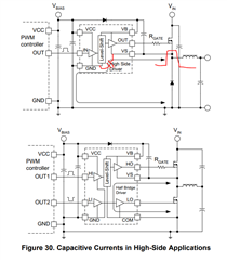
Thank you for asking. Figure 30 shows the parasitic capacitive current paths in 2 different configurations.
There is parasitic capacitance between the components due to the conductive elements being so close to each other and having different voltages. When the voltage changes during switching this causes a small amount of current since I = C * dV/dt. The path this current takes is marked by the arrows and is highlighted. This issue can be reduced by changing how the device is references to ground.
If you have any further questions, feel free to reach out.
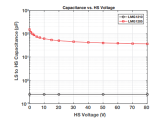
There are a variety of small, parasitic capacitances within the die and in different circuitry (such as the bootstrap diode). Any parasitic capacitance connected to the HS node, will experience a noticeable dv/dt. I = C * dv/dt, so current will flow in these parasitics capacitances. I recommend reading this document. Its for GaN drivers, but it shows the significance of the internal HS to LS capacitance:
Basically, having an extra connection to power ground could help reduce this current from causing ground bounce on the signal ground. The main half-bridge driver this applies to is UCC27714, which has these two pins. Isolated drivers basically achieve the same thing, and it is partly why they have better noise immunity.