This thread has been locked.

If you have a related question, please click the "Ask a related question" button in the top right corner. The newly created question will be automatically linked to this question.

UCC27714: H-bridge drive

Part Number: UCC27714

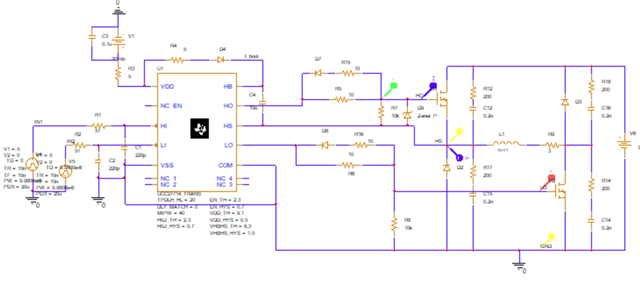
Figure 1 is my simulation schematic

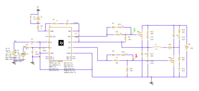
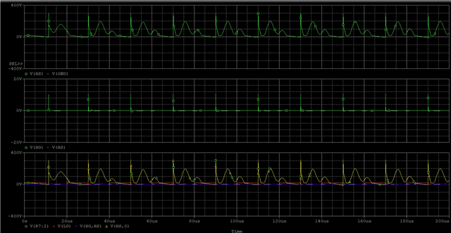
Figure 2 shows the HO and LO output waveforms

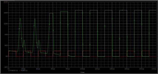
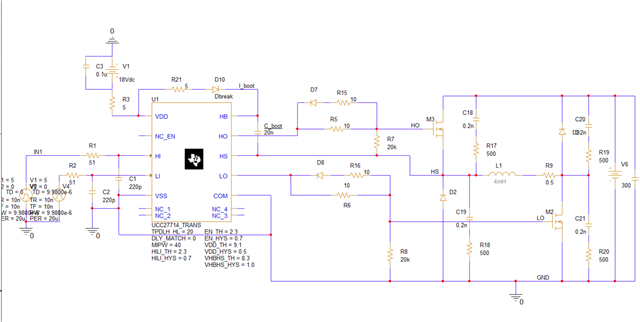
Figure 3 shows the driving waveforms of HO and LO when I increase the H-bridge supply voltage to 300V

I want to drive load L1 through the H-bridge, but the drive waveform is distorted on the high side.

At the same time, I wanted a faster current response, so when I tried to increase the H-bridge supply voltage, the drive waveform on the high side was completely deformed.

What adjustments I need to make,Hope for your help.

  • Hello XX Gu,

    For the HO output, it looks like the plot is showing the HO to ground signal. To see what the actual HO gate drive signal to the Mosfet is, can you plot the H0-HS differential voltage?

    Also plot the HS to ground on a separate signal, to see the waveform of the switch node. 

    Regards,

  • Hello Richard Herring,

    Thank you for your reply,When I opened the simulation software again, the supply voltage was 150V, and the simulation results seemed to be normal again,like this

    But when I raised the supply voltage to 300V again, it didn't seem to work again.

    Here are my schematics and simulations.

    Regards,

  • Hello XX Gu

    I am thinking that likely the switch node is not transitioning to ground, maybe for not long enough time, for the boot capacitor to charge in the higher line condition.

    Can you confirm if the HB-HS bias is staying above the recommended voltage (9V) in the higher input voltage operation?

    Can you plot HB-HS, and show the LO output? If you are switching LO, that will force the switch node to close to ground and allow the boot capacitor to charge and maintain the HB-HS bias.

    Regards,

  • Hello Richard Herring,

    I think you're right,It may have taken too long to charge the boot capacitor.

    Through the following calculations, I changed the boot capacitor to 20nf

    And it looks good, like this:

    My new question is, is the part I selected in the red box due to boot capacitor (C4)charging in the initial stage?

    Another question is what adjustments I need to make to the blue box selection.

    This is my schematic:

    What confused me was that I couldn't reproduce the previous output waveform Joy.

    Regards,

  • Hello,

    Good that you found a basic issue and resolved it. I would increase the boot capacitor a bit to accommodate the total gate charge, maybe increase to 33nF.

    The waveform you are showing of HO falling looks like HO to ground, which will have the switch node voltage (HS) as well. The fall time is what you are seeing on the HS waveform. This falling time will be dependent on the power train parameters and load condition. The falling time of the switch node will be dependent on the current flowing in the inductor and the total capacitance on the HS or switch node. I see that you have snubber capacitors, C18-21, this is likely affecting the switch node falling time. Also more current flowing in the inductor will result in the switch node falling faster. The current in the inductor will be the current that will determine the slew rate with the basic I= C dV/dt relationship. Higher current, or reduced capacitance will result in a faster fall time.

    Regards,

  • Hello,

    Thanks for your advice,I'm going to see it in action.