Other Parts Discussed in Thread: UCC21750, UCC12050, UCC21551
Hello everyone,
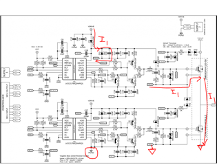
I'm working on a half-bridge circuit with a booster using UCC21755-Q1. However, I'm having issues with the usage of VEE (Negative supply rail) and DESAT. To avoid confusion, I will try to explain the design problem I'm facing in separate sections.
DESAT ISSUE
Considering that we will be using the 2MBI300VH-120-50 IGBT module and a +15V high drive voltage, according to the IGBT's technical documentation, we require a 7~8 volt DESAT threshold. However, the UCC21755-Q1 has a 5V DESAT threshold voltage. Subtracting the voltage drop across the resistor and diode, we obtain an approximate threshold level of 3.4V. This is not sufficient.
Q1: Can you suggest a method to increase the DESAT threshold level? (Different Device Maybe)
Q2: Could you provide any design recommendations or tips?
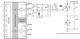
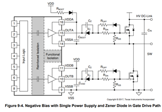
VEE ISSUE

Obtaining a negative gate voltage for the Low-Side driver is relatively easy, but I am struggling to apply a similar approach for the High-Side.
Q3: Can you suggest a method for applying a negative gate voltage to the high-side driver?
Q4: Do you have any suggestions or warnings regarding the design of the driver section shown in the Figure?
Best Regards,