This thread has been locked.

If you have a related question, please click the "Ask a related question" button in the top right corner. The newly created question will be automatically linked to this question.

TPS23770: Problem with TPS23770 circuit

Part Number: TPS23770
Other Parts Discussed in Thread: TPS23750, TPS23750EVM-107, TLV431

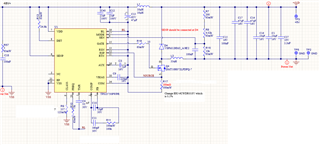
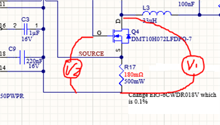
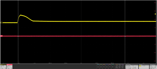
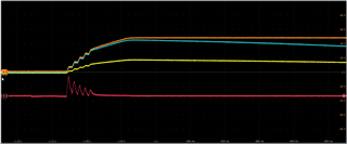
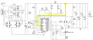
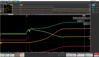
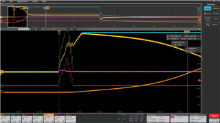
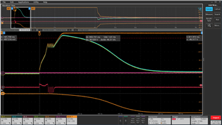
I modified the circuit on page 33 with a different switching mosfet and a different diode. For some reason I'm getting 38V or 40V on the output. I did my own layout.

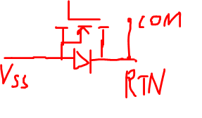
One error I found SENP is not attached to the diode on the layout, I don't think this would be a problem since SENP is higher than SEN.

  • Hi Steven,

    Thanks for reaching out.

    - Could you confirm you measured the output voltage between +5VD-TP5, instead of +5VD-Vss or +5VD-COM?

    - It is better to tie SENP with +5VD. L1 may cause some influence to SENP pin.

    - Could you share the datasheet of L3? Sometimes the inductor get saturated and is not sufficient enough for storing energy for a converter.

    Best regards,

    Diang

  • Datasheet for inductor: https://products.sumida.com/products/pdf/125CDMCCDS%20(en).pdf

    - Could you confirm you measured the output voltage between +5VD-TP5, instead of +5VD-Vss or +5VD-COM?

    Measured between TP3 and TP5 which is +5V and COM

    I'll try blue wiring SENP.

  • Hi Steven,

    Thanks for your reply. The inductor looks enough.

    "Measured between TP3 and TP5 which is +5V and COM", do you mean TP3 - TP5 is +5V? If so, I think it means the Buck converter regulating voltage is correct. The output of this Buck has a different ground with the TPS23770's COM pin.

    Best regards,

    Diang

  • TP3 to TP5 is 38V, I even swapped R8 and R15 and had the same result (the output voltage did not change still 38V). I also wired SENP to D4 with no good result. Is Q4 (the switch) a good part to use for this application (its a DMT10H072LFDFQ-7).  Are there any requirements for L1?

  • Hi Steven,

    Thanks for the updates. 

    - Q4 (DMT10H072LFDFQ-7) is 100-V and 62-mOhm. It looks good to me.

    - SENP is better to connected with the positive rail where the Vout refer to. I feel it is better to be after L1 as shown in the datasheet P33. I am not sure if L1 location can cause malfunction of SENP. While I think we could try to let SENP bypass the L1 to see if it helps. 

    Do you have the waveforms of MOSFET's Vds and Vgs? We could see if we can find some clues from the duty cycle and turn-off drain voltage.

    Best regards,

    Diang


  • Yellow is V1, and Red is the gate. The gate never really starts switching.

    The drain goes up to about 48V from the moment it's switched on and then resides at ~8V above the common voltage point.

  • Hi Steven,

    Thanks for your waveforms.

    We could see that the FET is not turning on. The issue could be the error amplifier to regulate the Vout did not work functionally.

    I may take some extra time to look though the blocking diagram and I will get back to you in 1-3 bossiness days.

    Best regards,

    Diang

  • Thanks I used a new TPS23750PWR and put it on to make sure it wasn't burned out. I had some switching on power up, but then it stops.

    The yellow trace is V1 the red is V2 (gate) and the orange is +5 (marked on the schematic) blue is ground (marked on the schematic)

  • Hi Steven,

    Thanks for the additional information.

    +5 should be the dc bus voltage and gnd should equals "dc bus" - "5 V". While there is no correct PWM control here. I need some time to take a look on the PWM controller's blocking diagram. Will reply you later.

    Best regards,

    Diang

  • Hi Steven,

    Besides, TPS23750EVM-107 is a Buck-Converter Evaluation Board. TPS23750 and TPS23770 are similar chip mainly has UVLO difference. 

    I will take a look on its test report to find the clues. 

    https://www.ti.com/lit/ug/slvu136a/slvu136a.pdf?ts=1689978711597&ref_url=https%253A%252F%252Fwww.ti.com%252Ftool%252FTPS23750EVM-107

    Best regards,

    Diang

  • It seems I have very slow switching when compared to the DEV board, I am not sure why. I do have a very good layout so I'm certain it's not that. One thing I did was start playing around with loop compensation and it switches more but still does not get the correct voltage. I have been looking for information on how to compensate the loop and there is none in the documentation. The diagram on page 34 is insufficient to compensate the loop.

  • Hi Steven,

    Sorry that I am still looking into this question.

    Between the SENP and Vout there is an inductor which is not for switching purpose. I try to check whether it is correct.

    Best regards,

    Diang

  • Hi Steven,

    TPS23750EVM-107 could be similar to your design and it should passed the Bode test. I think its compensation RC parameters can be refereed for your case. I can reach out to the FAE of your company to request a TPS23750EVM-107 sample for your to compare with your design.

    I am wondering if you could get some more information:

    Could you measure the voltage of COMP to RTN? This voltage should directly relate to the gate duty cycle.

    And the voltage of AUX to RTN? This voltage should be the positive rail of the gate drive. When gate is on, Vgs should close to AUX-RTN.

    I am still try to find the difference if SENP's connection,

    When using TLV431 as error amplifier and voltage translator is not needed:

    When using internal error amplifier and voltage translator is used:

    Best regards,

    Diang

  • Yeah, a sample would be nice to have for comparison. I checked the voltage on L1 and it is the same on either side as there is little or no current flowing through it. I have tried SENP on either side of L1 and it doesn't work. The problem I get now is the circuit starts to switch and then after about 10msec the

    This is what it looks like if I tie the scope ground to the COM of the TPS23750:


    The blue and yellow are +5V and Ground of the output, The orange is the difference between the two (should regulate to 5V, goes to 40V), the red is the gate drive or GATE, and the yellow is the source of the driver or the bottom of the diode). It looks like the device turns on, and then fails to regulate, why it goes to 40V I'll never know.

    This is what it looks like if I tie the scope ground to the GROUND of the power supply (Vin-)


    So again same thing but the supply is tied to power supply or input ground.

    The blue and yellow are +5V and Ground of the output, The orange is the difference between the two (should regulate to 5V, goes to 40V), the red is the gate drive or GATE, and the yellow is the source of the driver or the bottom of the diode).

    I also put a probe on BL/COM to see what it is doing, that is the green trace. It looks like it turns on and then drives COM in the wrong direction.

  • Hi Steven,

    Thanks for your test!

    Do you use a differential probe or all passive probes? I will look into the waveforms at different grounds tomorrow and get back to you.

    For the TPS23750EVM-107 sample. I just sent an email to the field team. Darren or Love may reach out to you in email early next week (field applications engineer is in vacation now). 

    Best regards,

    Diang

  • Thanks, After looking at it I think my BL/COM line is floating (green line), it should be the same potential as GND and not floating up. I don't understand why it would be moving up and not staying at the input  ground potenital

  • Hi Steven,

    Yes, the test results at different grounds look a little confusing to me too...

    Gate - com must be a 0-V (when gate is turning off) or a positive voltage (when gate is turning on). It looks strange that Gate-com is negative.  

    And when you are talking about the GROUND of the power supply (Vin-), do you mean it is VSS voltage? If so, this voltage should be very close to the COM voltage when the PD's internal hotswap between VSS and RTN turns on. Then there should be almost no difference when you using COM or VSS as ground reference.

    You may try to measure the body diode between Vss-RTN, and check the connection between COM and RTN to diagnose the ground issue.

    Best regards,

    Diang

  • I checked the diode on the FET and the pinout, it looks good. One issue I'm having now is I turned the board over (its double sided) and checked the circuit to see where all the power is being dissipated. R9 is hot (50C) and the board is drawing 150mA (would think it should be under, I think most of that is being dissipated into R9 (classification resistor). I am powering it from a bench supply so I guess I have to attach the bench supply to COM and not VSS? Can I power the 48V with a bench supply?

    I also changed the diode to the same one on the eval board (6CWQ10FN) and got this, it never really starts switching, it toggles a bit. The COM line (yellow) behaves differently.


  • Hi Steven,

    Thanks for your reply. Have you get the help to order of a TPS23750EVM-107 evaluation board?

    For bench power supply you can connect 48V - VSS, then the TPS23770 can have the inrush current limitation. 

    For R9 and classification. You should see 10-V at CLASS pin when VDD - VSS is 11.3 - 21.28 V. When you apply a higher voltage, CLASS voltage should be 0V according to the blocking diagram. 

    Best regards,

    Diang

  • Yeah, the eval board should be coming. Shouldn't the classification stop if I apply 48V with the bench supply? The resistor is 50C so it's burning up a lot of power, which also means CLASS is high at 48V. Another problem is the regulator never starts switching, why is it not starting?

  • Hi Steven,

    If VDD-VSS is 48V, theoretically CLASS should stop and you should not see 10-V between CLASS-VSS. You can check it on your board.

    For the regulator issue, sorry that I did not find wrong circuit design from your schematic. Do you think it is workable to test the TPS23750EVM-107 evaluation board to see if it can fit your system? If so, you can replace the existing circuit by the TPS23750EVM-107's circuit in your system (TPS23750 and TPS23770 are similar chip mainly has UVLO difference).

    Best regards,

    Diang

  • Hi Steven,

    I will close this thread for now. Please reply or open a new thread if you have further questions after you tested the EVM we shipped to you.

    Best regards,

    Diang