This thread has been locked.

If you have a related question, please click the "Ask a related question" button in the top right corner. The newly created question will be automatically linked to this question.

Shut down modes of TPS65131

Other Parts Discussed in Thread: TPS65131, TPS65130

When I put a moderately high load on the TPS65131 (75ma +/- 15v with 5v in), my circuit begins to shut down after 80ms or so. The peak voltage at INp begins to drop from 15V or so to 7 volts and the frequency of the pulses changes from 215ns wide pulses 720ns apart to 730ns 50% duty cycle pulses. The outputs change from +/-15v to +4.8 and -20v respectivley.

I was expecting to be able to operate the circuit at 150ma normal with some short duration peaks to maybe 250ma. I calculated using equation (3) from the datasheet that with 250ma IOUTp, Ilp would be 1.17A. Figure 31 implies I can run this chip out to 500ma or so, with appropriate inductors. The rated current on the 4.7uH inductors I selected is 1.1A.

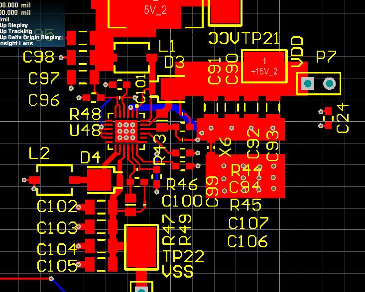
At 40ma load the circuit works fine.  I am using the power-save mode and I wonder if that might be part of the problem...the circuit not working when not in power save mode. Can you tell from thie behavior what operating/shut down mode the device is going into? I've attached the schematic and board layout.

3051.Power Supply Page.pdf

  • The only automatic shutdown mode is thermal shutdown but you are no where near that threshold for the power levels you are describing.  Is the reference voltage staying within regulation with the increased capacitor:

    If so, then most likely the issue is with the board layout.  The output feedback pins OUTx and FBx are very sensitive to switching noise.  Unless the board is laid out very tight, like the TPS65131EVM, the switching noise couples in and false trips the current limit circuitry.  This can cause the outputs to be power limited and would explain the +4.8V on the +15V.  However, it does not explain the -20V on the negative rail.  As shown in datasheet Figure 37, the negative rail can float low at very light load if the IC is running in PWM mode.  PFM mode prevents this from happening.

    I suggest that you order an EVM, modify it for your components and retest the EVM.  If the EVM works, then the problem is definitely with the board layout.

  • VRef is staying at 1.2 volts throughout the startup and 'shutdown'. I'm seeing 1.5v p-p bursts on VRef that last 40ns or so every 360ns and they don't really change much from when the outputs are correct to where they fall out of regulation. The FBP line has 40ns long 500mv p-p bursts and the bursts on the FBN line are closer to 1v p-p. OUTN has about 4 volts of overshoot and undershoot on its switching pulses. Is this enough to cause problems do you think? I'll take a look at the EVM layout and compare it to ours and will take a look at ordering the EVM.


    Thanks,


    Chuck


  • Hello Chuck,

    It could happen that the part is not able to work if there is noise coupling into the feedback, vref or Cx lines. Please review the EVM layout and if you generate a layout which is close to the EVM layout, the converter should work.

    Best regards,
    Brigitte

  • I was able to get the EVM board last week and modify the components to match my design and verify proper voltage output under load. And as suspected it worked, although I don't seem to be getting quite the Vneg I expect from the calculations but need to dig into that matter. That pretty much confirms that the layout was the issue. What concerns me is that while I can much much closer to the EVM layout than I am now, I'm not sure I can match it 100% and it seems hard to predict the effect of that and I only want to do one more board turn. I certainly understand that switching power supplies are very trick but it feels to me as though this part is too sensitive to layout IMHO.

    But thanks for the support because otherwise I would have had no idea what to try next!

  • Hello Chuck,

    The most important pins on this part are the feedback pins, the compensation pins and the reference voltage pin. If you can match the layout there, this is already very helpful. In addition, always keep in mind to minimize the high current loops then the part should work properly.

    Especially with converters switching above 1MHz, layout is always tricky.

    How did you calculate the negative voltage and what voltage do you get?

    Best regards,
    Brigitte

  • Thanks, I figured those are the most critical, and I think I can get very close to the same layout, though I do have some questions on the grounding scheme used which I'll discuss later in the message.

    I'm using formula (2) from the data sheet. I modifed the EVM so that R4 is 178K and R3 is 2.1M. This should give me -14.311 volts. I actually want -15v but we couldn't find a 2.2M for R3. I was getting 13.9 which is 2.4% low. It's certainly possible that the actual 1% resistor values were off in the worst case to give me that 2.4% error, but I'd be surprised. It's not critical though.

    I want to establish an "analog ground" for the +/-15v supplies at one point relative to the "digital" ground for the 5V supply which is my input to the TPS65131. However, the schematic for the EVM shows the same ground for input and ouptuts (solid triangle) and  a separate ground (horiz lines) for the Vpos and Vneg dividers, AGND pin and also for the jumper options. I haven't worked through the EVM layout yet to see where those two grounds are connected but the schematic shows they are.

    My current design 5100.Power Supply Page.pdf has analog ground connected to PGND pins 2 and 3, and is used for C5 and C8 and the outputs capacitors. This net is tied to AGND only at pin 19 and AGND used for the dividers, the thermal pad, and all input caps, C1-4. I wonder if my change to the grounding scheme is partially the problem and how I wold resolve it? I guess a "third" ground path, equivalent to your horizontal line symbol ground layed out per the EVM, then use another ground path for my output capaictors and the remainder of my analog circuitry tied at one point to PGND and not to AGND except where it is tied to PGND per the EVM.


    Thanks again,


    Chuck

  • Working on the layout and I have a question around R7, the zero-ohm resistor. Is this there so that a resistor can be put in series with C8 or is it there for layout reasons? If not then it appears that 87 could go right from pin 18 to AGND and the AGND area between the via near pin 19 and C8 down to C7 could be filled in. it actually looks like the left side pad for C8 bridges the AGND island where the via is and the AGND land that runs along C8, R7, C7 and R2 on the right and then ghoes up over the top to connect to C5 and shields C5 and R8 over towards  C6. I wouldn't think that the impedence change that would occur in making this all one "AGND land mass" would have much effect but it gets back to the function of R7.


    Thanks,


    Chuck

  • R7 is a place holder for a larger 10k-100k ohm resistor used to reduce noise coupling.  The paragraph under datasheet equation 12 mentions this.  I found that the EVM, with its very tight layout, did not need this resistor.

  • Thanks. I hope I'm not belaboring the point, and I see that the ref desgs on the TPS65130 datasheet and those on the EVM datasheet are different. I was referring to R7 (and R8 for that matter) on the EVM datasheet schematic which is not shown on the TPS65130 datasheet on page 23. They are in series with the caps on the Cn and Cp lines to ground.

    I think the feedforward bandwidth limting resistors you are referring to after equation 12 are R8 and R9 yes? They aren't mentioned explicility by ref des anywhere in the text. I am using 100K resistors on both rails for my design.

  • Hello Chuck,

    Neither the series resistors to the feedforward capacitors nor the ones in CP and CN are necessary components. Sometimes when the load transient response of the standard circuit suggestion is not good enough you can add the one or the other of these resistors to increase the bandwidth of the converter, but I would start with 0R resistors there and check if the converter reacts fast enough on the worst case load transient. Just if this is not the case, you can start to add higher resistance to these resistors to increase the bandwidth, but most systems do not need them.

    Best regards,
    Brigitte