This thread has been locked.

If you have a related question, please click the "Ask a related question" button in the top right corner. The newly created question will be automatically linked to this question.

UCC2801: output PWM isn't regulated

Part Number: UCC2801

Dear TI team,

We are using the ucc2801 as boost driver for 10 years now as a DIP version. As this is becomng obsolete, we moved to the SOIC version thus making a pcb modification .
We mainly have to boards running with this component ; one is made to step up a 24V battery to 28V, the other one fro ma 48V battery to 56V.

The pcb are identical on both boards. The 56 V version is working just fine.

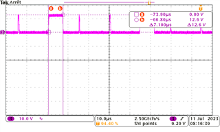
However, on the 28V version with the new package, it seems like the UCC2801 doesn't manage to output a duty different thtan 50% or 0%. It does regulate but it does the job by pushing hard then relax and so ON. I am joining a picture to explain this...


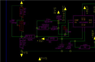
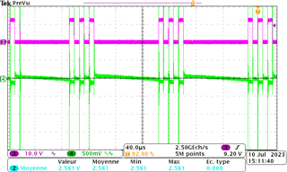
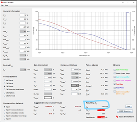
We have been playing with the capacitors around the COMP pin (see the schematic attached) but I could not find why the behaviour.  WOuld you have any suggestions ?

Best regards,

TOURNON Edgar

  • Hi Edgar.

    I checked your compensator values between FB and COM pins and I noticed that you might have selected incorrect values. You might be facing an instability issue. This is a type II compensator where the idea is to increase the low frequency gain and have an appropriate crossover frequency in order to have a decent closed loop regulation and fast response against transients or perturbations in the system.


    To do this I recommend the following: (please follow the same reference name of your squematic)
    -Select a crossover frequency of 1/10 of switching frequency (fc=fs/10).
    -Select the shorter corner frequency of your compensation 1/10 of crossover over frequency (f1=fc/10=1/(2*pi*R10*C13)). This will prevent reducing the phase margin and therefore keeping the system stable.
    -Select the higher corner frequency 10 times or more the shorter corner frequency (f2=10*f1=1/(2*pi*R10*C11)). This will keep the magnitude of the loop gain in good shape and prevent any stability issues. You can just make C11=C13/10. The idea is that C11<<C13.

    Checking your schematic, C11>>C13 (the opposite). I simulated you closed loop gain and phase response (see attached) and the crossover frequency is too short (fc=230Hz). Something you can do is just switch positions of C11 and C13 and check if it works. Or you would redesign your compensator following the recommendations above.

  • Hi Manuel,

    I have first been trying to invert C11& C13 without any success.
    I have done the calculation you provde and have found R10 was to high so I did reduce it to the calculated value 28k without succes. 
    There are many component mounted around this IC so we did try to modify/remove most of them without success.

    However, depending on the mounted components and on values, we sometimes get the following behavior :

    Do you know if this one is normal (I guess not as other boards don't do this). Indeed, the IC is doiing full power (duty =50%) then a certain amount of emty pulses and again . THis provides the 28V output but increase the ripple. Do you have any idea why the IC would skip pulse/ be instable ...

  • Hi Edgar.

    Please, see attached a recommended design for your compensator (Current Mode Control Boost). As you can see, the loop gain has a crossover frequency of around fc=10KHz and a phase margin of around 77 degrees. (Phase Margin=180-fco)

    R10=28Kohms, C13=200pF, C11=20pF